SPRSP93 November 2024 F29H850TU , F29H859TU-Q1
ADVANCE INFORMATION
- 1
- 1 Features
- 2 Applications
- 3 Description
- 4 Device Comparison
- 5 Pin Configuration and Functions
-
6 Specifications
- 6.1 Absolute Maximum Ratings
- 6.2 F29H85x ESD Ratings – Commercial
- 6.3 F29H85x ESD Ratings – Automotive
- 6.4 F29P58x ESD Ratings – Commercial
- 6.5 F29P58x ESD Ratings – Automotive
- 6.6 Recommended Operating Conditions
- 6.7 Power Consumption Summary
- 6.8 Electrical Characteristics
- 6.9 Thermal Resistance Characteristics for ZEX Package
- 6.10 Thermal Resistance Characteristics for PTS Package
- 6.11 Thermal Resistance Characteristics for RFS Package
- 6.12 Thermal Resistance Characteristics for PZS Package
- 6.13 Thermal Design Considerations
- 6.14
System
- 6.14.1
Power Management Module (PMM)
- 6.14.1.1 Introduction
- 6.14.1.2 Overview
- 6.14.1.3 External Components
- 6.14.1.4 Power Sequencing
- 6.14.1.5 Power Management Module Electrical Data and Timing
- 6.14.2 Reset Timing
- 6.14.3
Clock Specifications
- 6.14.3.1 Clock Sources
- 6.14.3.2
Clock Frequencies, Requirements, and Characteristics
- 6.14.3.2.1
Input Clock Frequency and Timing
Requirements, PLL Lock Times
- 6.14.3.2.1.1 Input Clock Frequency
- 6.14.3.2.1.2 XTAL Oscillator Characteristics
- 6.14.3.2.1.3 X1 Input Level Characteristics When Using an External Clock Source Not a Crystal
- 6.14.3.2.1.4 X1 Timing Requirements
- 6.14.3.2.1.5 AUXCLKIN Timing Requirements
- 6.14.3.2.1.6 APLL Characteristics
- 6.14.3.2.1.7 XCLKOUT Switching Characteristics PLL Bypassed or Enabled
- 6.14.3.2.1
Input Clock Frequency and Timing
Requirements, PLL Lock Times
- 6.14.3.3 Input Clocks
- 6.14.3.4 XTAL Oscillator
- 6.14.3.5 Internal Oscillators
- 6.14.4 Flash Parameters
- 6.14.5 Memory Subsystem (MEMSS)
- 6.14.6 Debug/JTAG
- 6.14.7 GPIO Electrical Data and Timing
- 6.14.8 Real-Time Direct Memory Access (RTDMA)
- 6.14.9 Low-Power Modes
- 6.14.10
External Memory Interface (EMIF)
- 6.14.10.1 Asynchronous Memory Support
- 6.14.10.2 Synchronous DRAM Support
- 6.14.10.3
EMIF Electrical Data and Timing
- 6.14.10.3.1 EMIF Synchronous Memory Timing Requirements
- 6.14.10.3.2 EMIF Synchronous Memory Switching Characteristics
- 6.14.10.3.3 EMIF Synchronous Memory Timing Diagrams
- 6.14.10.3.4 EMIF Asynchronous Memory Timing Requirements
- 6.14.10.3.5 EMIF Asynchronous Memory Switching Characteristics
- 6.14.10.3.6 EMIF Asynchronous Memory Timing Diagrams
- 6.14.1
Power Management Module (PMM)
- 6.15
C29x Analog Peripherals
- 6.15.1 Analog Subsystem
- 6.15.2
Analog-to-Digital Converter (ADC)
- 6.15.2.1 ADC Configurability
- 6.15.2.2
ADC Electrical Data and Timing
- 6.15.2.2.1 ADC Operating Conditions 12-bit Single-Ended
- 6.15.2.2.2 ADC Operating Conditions 12-bit Differential
- 6.15.2.2.3 ADC Operating Conditions 16-bit Single-Ended
- 6.15.2.2.4 ADC Operating Conditions 16-bit Differential
- 6.15.2.2.5 ADC Timing Requirements
- 6.15.2.2.6 ADC Characteristics 12-bit Single-Ended
- 6.15.2.2.7 ADC Characteristics 12-bit Differential
- 6.15.2.2.8 ADC Characteristics 16-bit Single-Ended
- 6.15.2.2.9 ADC Characteristics 16-bit Differential
- 6.15.2.2.10 ADC INL and DNL
- 6.15.2.2.11 ADC Input Model Models
- 6.15.2.2.12 ADC Timing Diagrams
- 6.15.3 Temperature Sensor
- 6.15.4 Comparator Subsystem (CMPSS)
- 6.15.5 Buffered Digital-to-Analog Converter (DAC)
- 6.16
C29x Control Peripherals
- 6.16.1 Enhanced Capture (eCAP)
- 6.16.2 High-Resolution Capture (HRCAP)
- 6.16.3 Enhanced Pulse Width Modulator (ePWM)
- 6.16.4 External ADC Start-of-Conversion Electrical Data and Timing
- 6.16.5 High-Resolution Pulse Width Modulator (HRPWM)
- 6.16.6 Enhanced Quadrature Encoder Pulse (eQEP)
- 6.16.7 Sigma-Delta Filter Module (SDFM)
- 6.17
C29x Communications Peripherals
- 6.17.1 Modular Controller Area Network (MCAN)
- 6.17.2 Fast Serial Interface (FSI)
- 6.17.3 Inter-Integrated Circuit (I2C)
- 6.17.4 Power Management Bus (PMBus) Interface
- 6.17.5 Serial Peripheral Interface (SPI)
- 6.17.6 Single Edge Nibble Transmission (SENT)
- 6.17.7 Local Interconnect Network (LIN)
- 6.17.8 EtherCAT SubordinateDevice Controller (ESC)
- 6.17.9 Universal Asynchronous Receiver-Transmitter (UART)
-
7 Detailed Description
- 7.1 Overview
- 7.2 Functional Block Diagram
- 7.3 Error Signaling Module (ESM_C29)
- 7.4 Error Aggregator
- 7.5
Memory
- 7.5.1 C29x Memory Map
- 7.5.2
Flash Memory Map
- 7.5.2.1 Flash MAIN Region Address Map (F29H85x, 4MB)
- 7.5.2.2 Flash MAIN Region Address Map (F29H85x, 2MB)
- 7.5.2.3 Flash MAIN Region Address Map (F29P58x, 4MB)
- 7.5.2.4 Flash MAIN Region Address Map (F29P58x, 2MB)
- 7.5.2.5 Flash MAIN Region Address MAP (F29P58x, 1MB)
- 7.5.2.6 Flash Data Bank Address Map
- 7.5.2.7 Flash BANKMGMT Region Address Map
- 7.5.2.8 Flash SECCFG Region Address Map
- 7.5.3 Peripheral Registers Memory Map
- 7.6 Identification
- 7.7 Boot ROM
- 7.8 Security Modules and Cryptographic Accelerators
- 7.9
C29x Subsystem
- 7.9.1 C29 CPU Architecture
- 7.9.2 Peripheral Interrupt Priority and Expansion (PIPE)
- 7.9.3 Data Logging and Trace (DLT)
- 7.9.4 Waveform Analyzer Diagnostics (WADI)
- 7.9.5 Embedded Real-Time Analysis and Diagnostic (ERAD)
- 7.9.6 Inter-Processor Communications (IPC)
- 7.9.7 Watchdog
- 7.9.8 Dual-Clock Comparator (DCC)
- 7.9.9 Configurable Logic Block (CLB)
- 7.10 Lockstep Compare Module (LCM)
- 8 Applications, Implementation, and Layout
- 9 Device and Documentation Support
- 10Revision History
- 11Mechanical, Packaging, and Orderable Information
パッケージ・オプション
デバイスごとのパッケージ図は、PDF版データシートをご参照ください。
メカニカル・データ(パッケージ|ピン)
- PZS|100
- PTS|176
- RFS|144
- ZEX|256
サーマルパッド・メカニカル・データ
発注情報
6.17.2.2 FSI Receiver
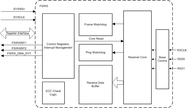
The receiver module interfaces to the FSI clock (RXCLK), and data lines (RXD0 and RXD1) after they pass through an optional programmable delay line. The receiver core handles the data framing, CRC computation, and frame-related error checking. The receiver bit clock and state machine are run by the RXCLK input, which is asynchronous to the device system clock.
The receiver control registers let the CPU program, control, and monitor the operation of the FSIRX. The receive data buffer is accessible by the CPU, and the DMA.
The receiver core has the following features:
- 16-word data buffer
- Multiple supported frame types
- Ping frame watchdog
- Frame watchdog
- CRC calculation and comparison in hardware
- ECC detection
- Programmable delay line control on incoming signals
- DMA support
- SPI compatibility mode
Figure 6-69 shows the FSIRX CPU interface. Figure 6-70 provides a high-level overview of the internal modules present in the FSIRX. Not all data paths and internal connections are shown.
 Figure 6-69 FSIRX CPU Interface
 Figure 6-70 FSIRX Block Diagram