SPRSP93 November   2024 F29H850TU , F29H859TU-Q1

ADVANCE INFORMATION  

  1.   1
  2. Features
  3. Applications
  4. Description
    1. 3.1 Functional Block Diagram
  5. Device Comparison
    1. 4.1 Related Products
  6. Pin Configuration and Functions
    1. 5.1 Pin Diagrams
    2. 5.2 Pin Attributes
    3. 5.3 Signal Descriptions
      1. 5.3.1 Analog Signals
      2. 5.3.2 Digital Signals
      3. 5.3.3 Power and Ground
      4. 5.3.4 Test, JTAG, and Reset
    4. 5.4 Pins With Internal Pullup and Pulldown
    5. 5.5 Pin Multiplexing
      1. 5.5.1 GPIO Muxed Pins
    6. 5.6 Connections for Unused Pins
  7. Specifications
    1. 6.1  Absolute Maximum Ratings
    2. 6.2  F29H85x ESD Ratings – Commercial
    3. 6.3  F29H85x ESD Ratings – Automotive
    4. 6.4  F29P58x ESD Ratings – Commercial
    5. 6.5  F29P58x ESD Ratings – Automotive
    6. 6.6  Recommended Operating Conditions
    7. 6.7  Power Consumption Summary
      1. 6.7.1 System Current Consumption VREG Enabled
      2. 6.7.2 System Current Consumption VREG Disable - External Supply
      3. 6.7.3 Operating Mode Test Description
      4. 6.7.4 Reducing Current Consumption
        1. 6.7.4.1 Typical Current Reduction per Disabled Peripheral
    8. 6.8  Electrical Characteristics
    9. 6.9  Thermal Resistance Characteristics for ZEX Package
    10. 6.10 Thermal Resistance Characteristics for PTS Package
    11. 6.11 Thermal Resistance Characteristics for RFS Package
    12. 6.12 Thermal Resistance Characteristics for PZS Package
    13. 6.13 Thermal Design Considerations
    14. 6.14 System
      1. 6.14.1  Power Management Module (PMM)
        1. 6.14.1.1 Introduction
        2. 6.14.1.2 Overview
          1. 6.14.1.2.1 Power Rail Monitors
            1. 6.14.1.2.1.1 I/O POR (Power-On Reset) Monitor
            2. 6.14.1.2.1.2 I/O BOR (Brown-Out Reset) Monitor
            3. 6.14.1.2.1.3 VDD POR (Power-On Reset) Monitor
          2. 6.14.1.2.2 External Supervisor Usage
          3. 6.14.1.2.3 Delay Blocks
          4. 6.14.1.2.4 Internal 1.2-V LDO Voltage Regulator (VREG)
          5. 6.14.1.2.5 VREGENZ
        3. 6.14.1.3 External Components
          1. 6.14.1.3.1 Decoupling Capacitors
            1. 6.14.1.3.1.1 VDDIO Decoupling
            2. 6.14.1.3.1.2 VDD Decoupling
        4. 6.14.1.4 Power Sequencing
          1. 6.14.1.4.1 Supply Pins Ganging
          2. 6.14.1.4.2 Signal Pins Power Sequence
          3. 6.14.1.4.3 Supply Pins Power Sequence
            1. 6.14.1.4.3.1 External VREG/VDD Mode Sequence
            2. 6.14.1.4.3.2 Internal VREG/VDD Mode Sequence
            3. 6.14.1.4.3.3 Supply Sequencing Summary and Effects of Violations
            4. 6.14.1.4.3.4 Supply Slew Rate
        5. 6.14.1.5 Power Management Module Electrical Data and Timing
          1. 6.14.1.5.1 Power Management Module Operating Conditions
          2. 6.14.1.5.2 Power Management Module Characteristics
      2. 6.14.2  Reset Timing
        1. 6.14.2.1 Reset Sources
        2. 6.14.2.2 Reset Electrical Data and Timing
          1. 6.14.2.2.1 Reset XRSn Timing Requirements
          2. 6.14.2.2.2 Reset XRSn Switching Characteristics
          3. 6.14.2.2.3 Reset Timing Diagrams
      3. 6.14.3  Clock Specifications
        1. 6.14.3.1 Clock Sources
        2. 6.14.3.2 Clock Frequencies, Requirements, and Characteristics
          1. 6.14.3.2.1 Input Clock Frequency and Timing Requirements, PLL Lock Times
            1. 6.14.3.2.1.1 Input Clock Frequency
            2. 6.14.3.2.1.2 XTAL Oscillator Characteristics
            3. 6.14.3.2.1.3 X1 Input Level Characteristics When Using an External Clock Source Not a Crystal
            4. 6.14.3.2.1.4 X1 Timing Requirements
            5. 6.14.3.2.1.5 AUXCLKIN Timing Requirements
            6. 6.14.3.2.1.6 APLL Characteristics
            7. 6.14.3.2.1.7 XCLKOUT Switching Characteristics PLL Bypassed or Enabled
        3. 6.14.3.3 Input Clocks
        4. 6.14.3.4 XTAL Oscillator
          1. 6.14.3.4.1 Introduction
          2. 6.14.3.4.2 Overview
            1. 6.14.3.4.2.1 Electrical Oscillator
              1. 6.14.3.4.2.1.1 Modes of Operation
                1. 6.14.3.4.2.1.1.1 Crystal Mode of Operation
                2. 6.14.3.4.2.1.1.2 Single-Ended Mode of Operation
              2. 6.14.3.4.2.1.2 XTAL Output on XCLKOUT
            2. 6.14.3.4.2.2 Quartz Crystal
            3. 6.14.3.4.2.3 GPIO Modes of Operation
          3. 6.14.3.4.3 Functional Operation
            1. 6.14.3.4.3.1 ESR – Effective Series Resistance
            2. 6.14.3.4.3.2 Rneg – Negative Resistance
            3. 6.14.3.4.3.3 Start-up Time
            4. 6.14.3.4.3.4 DL – Drive Level
          4. 6.14.3.4.4 How to Choose a Crystal
          5. 6.14.3.4.5 Testing
          6. 6.14.3.4.6 Common Problems and Debug Tips
          7. 6.14.3.4.7 Crystal Oscillator Specifications
            1. 6.14.3.4.7.1 Crystal Oscillator Electrical Characteristics
            2. 6.14.3.4.7.2 Crystal Equivalent Series Resistance (ESR) Requirements
            3. 6.14.3.4.7.3 Crystal Oscillator Parameters
            4. 6.14.3.4.7.4 Crystal Oscillator Electrical Characteristics
        5. 6.14.3.5 Internal Oscillators
          1. 6.14.3.5.1 INTOSC Characteristics
      4. 6.14.4  Flash Parameters
        1. 6.14.4.1 Flash Parameters 
      5. 6.14.5  Memory Subsystem (MEMSS)
        1. 6.14.5.1 Introduction
        2. 6.14.5.2 Features
        3. 6.14.5.3 RAM Specifications
      6. 6.14.6  Debug/JTAG
        1. 6.14.6.1 JTAG Electrical Data and Timing
          1. 6.14.6.1.1 DEBUGSS Timing Requirements
          2. 6.14.6.1.2 DEBUGSS Switching Characteristics
          3. 6.14.6.1.3 JTAG Timing Diagram
          4. 6.14.6.1.4 SWD Timing Diagram
      7. 6.14.7  GPIO Electrical Data and Timing
        1. 6.14.7.1 GPIO – Output Timing
          1. 6.14.7.1.1 General-Purpose Output Switching Characteristics
          2. 6.14.7.1.2 General-Purpose Output Timing Diagram
        2. 6.14.7.2 GPIO – Input Timing
          1. 6.14.7.2.1 General-Purpose Input Timing Requirements
          2. 6.14.7.2.2 Sampling Mode
        3. 6.14.7.3 Sampling Window Width for Input Signals
      8. 6.14.8  Real-Time Direct Memory Access (RTDMA)
        1. 6.14.8.1 Introduction
          1. 6.14.8.1.1 Features
          2. 6.14.8.1.2 Block Diagram
      9. 6.14.9  Low-Power Modes
        1. 6.14.9.1 Clock-Gating Low-Power Modes
        2. 6.14.9.2 Low-Power Mode Wake-up Timing
          1. 6.14.9.2.1 IDLE Mode Timing Requirements
          2. 6.14.9.2.2 IDLE Mode Switching Characteristics
          3. 6.14.9.2.3 IDLE Entry and Exit Timing Diagram
          4. 6.14.9.2.4 STANDBY Mode Timing Requirements
          5. 6.14.9.2.5 STANDBY Mode Switching Characteristics
          6. 6.14.9.2.6 STANDBY Entry and Exit Timing Diagram
      10. 6.14.10 External Memory Interface (EMIF)
        1. 6.14.10.1 Asynchronous Memory Support
        2. 6.14.10.2 Synchronous DRAM Support
        3. 6.14.10.3 EMIF Electrical Data and Timing
          1. 6.14.10.3.1 EMIF Synchronous Memory Timing Requirements
          2. 6.14.10.3.2 EMIF Synchronous Memory Switching Characteristics
          3. 6.14.10.3.3 EMIF Synchronous Memory Timing Diagrams
          4. 6.14.10.3.4 EMIF Asynchronous Memory Timing Requirements
          5. 6.14.10.3.5 EMIF Asynchronous Memory Switching Characteristics
          6. 6.14.10.3.6 EMIF Asynchronous Memory Timing Diagrams
    15. 6.15 C29x Analog Peripherals
      1. 6.15.1 Analog Subsystem
        1. 6.15.1.1 Features
        2. 6.15.1.2 Block Diagram
        3. 6.15.1.3 Analog Pin Connections
      2. 6.15.2 Analog-to-Digital Converter (ADC)
        1. 6.15.2.1 ADC Configurability
          1. 6.15.2.1.1 Signal Mode
        2. 6.15.2.2 ADC Electrical Data and Timing
          1. 6.15.2.2.1  ADC Operating Conditions 12-bit Single-Ended
          2. 6.15.2.2.2  ADC Operating Conditions 12-bit Differential
          3. 6.15.2.2.3  ADC Operating Conditions 16-bit Single-Ended
          4. 6.15.2.2.4  ADC Operating Conditions 16-bit Differential
          5. 6.15.2.2.5  ADC Timing Requirements
          6. 6.15.2.2.6  ADC Characteristics 12-bit Single-Ended
          7. 6.15.2.2.7  ADC Characteristics 12-bit Differential
          8. 6.15.2.2.8  ADC Characteristics 16-bit Single-Ended
          9. 6.15.2.2.9  ADC Characteristics 16-bit Differential
          10. 6.15.2.2.10 ADC INL and DNL
          11. 6.15.2.2.11 ADC Input Model Models
          12. 6.15.2.2.12 ADC Timing Diagrams
      3. 6.15.3 Temperature Sensor
        1. 6.15.3.1 Temperature Sensor Electrical Data and Timing
          1. 6.15.3.1.1 Temperature Sensor Characteristics
      4. 6.15.4 Comparator Subsystem (CMPSS)
        1. 6.15.4.1 CMPSS Connectivity Diagram
        2. 6.15.4.2 Block Diagram
        3. 6.15.4.3 CMPSS Electrical Data and Timing
          1. 6.15.4.3.1 Comparator Electrical Characteristics
          2.        CMPSS Comparator Input Referred Offset and Hysteresis
          3. 6.15.4.3.2 CMPSS DAC Static Electrical Characteristics
          4. 6.15.4.3.3 CMPSS Illustrative Graphs
      5. 6.15.5 Buffered Digital-to-Analog Converter (DAC)
        1. 6.15.5.1 Buffered DAC Electrical Data and Timing
          1. 6.15.5.1.1 Buffered DAC Operating Conditions
          2. 6.15.5.1.2 Buffered DAC Electrical Characteristics
    16. 6.16 C29x Control Peripherals
      1. 6.16.1 Enhanced Capture (eCAP)
        1. 6.16.1.1 eCAP Block Diagram
        2. 6.16.1.2 eCAP Synchronization
        3. 6.16.1.3 eCAP Electrical Data and Timing
          1. 6.16.1.3.1 eCAP Timing Requirements
          2. 6.16.1.3.2 eCAP Switching Characteristics
      2. 6.16.2 High-Resolution Capture (HRCAP)
        1. 6.16.2.1 eCAP and HRCAP Block Diagram
        2. 6.16.2.2 HRCAP Electrical Data and Timing
          1. 6.16.2.2.1 HRCAP Switching Characteristics
          2. 6.16.2.2.2 HRCAP Figure and Graph
      3. 6.16.3 Enhanced Pulse Width Modulator (ePWM)
        1. 6.16.3.1 Control Peripherals Synchronization
        2. 6.16.3.2 ePWM Electrical Data and Timing
          1. 6.16.3.2.1 ePWM Timing Requirements
          2. 6.16.3.2.2 ePWM Switching Characteristics
          3. 6.16.3.2.3 Trip-Zone Input Timing
            1. 6.16.3.2.3.1 PWM Hi-Z Characteristics Timing Diagram
      4. 6.16.4 External ADC Start-of-Conversion Electrical Data and Timing
        1. 6.16.4.1 External ADC Start-of-Conversion Switching Characteristics
        2. 6.16.4.2 ADCSOCAO or ADCSOCBO Timing Diagram
      5. 6.16.5 High-Resolution Pulse Width Modulator (HRPWM)
        1. 6.16.5.1 HRPWM Electrical Data and Timing
          1. 6.16.5.1.1 High-Resolution PWM Characteristics
      6. 6.16.6 Enhanced Quadrature Encoder Pulse (eQEP)
        1. 6.16.6.1 eQEP Electrical Data and Timing
          1. 6.16.6.1.1 eQEP Timing Requirements
          2. 6.16.6.1.2 eCAP Switching Characteristics
      7. 6.16.7 Sigma-Delta Filter Module (SDFM)
        1. 6.16.7.1 SDFM Electrical Data and Timing
          1. 6.16.7.1.1 SDFM Electrical Data and Timing (Synchronized GPIO)
          2. 6.16.7.1.2 SDFM Electrical Data and Timing (Using ASYNC)
            1. 6.16.7.1.2.1 SDFM Timing Requirements When Using Asynchronous GPIO ASYNC Option
            2. 6.16.7.1.2.2 SDFM Timing Requirements When Using Synchronous GPIO SYNC Option
          3. 6.16.7.1.3 SDFM Timing Diagram
    17. 6.17 C29x Communications Peripherals
      1. 6.17.1 Modular Controller Area Network (MCAN)
      2. 6.17.2 Fast Serial Interface (FSI)
        1. 6.17.2.1 FSI Transmitter
          1. 6.17.2.1.1 FSITX Electrical Data and Timing
            1. 6.17.2.1.1.1 FSITX Switching Characteristics
            2. 6.17.2.1.1.2 FSITX Timings
        2. 6.17.2.2 FSI Receiver
          1. 6.17.2.2.1 FSIRX Electrical Data and Timing
            1. 6.17.2.2.1.1 FSIRX Timing Requirements
            2. 6.17.2.2.1.2 FSIRX Switching Characteristics
            3. 6.17.2.2.1.3 FSIRX Timings
        3. 6.17.2.3 FSI SPI Compatibility Mode
          1. 6.17.2.3.1 FSITX SPI Signaling Mode Electrical Data and Timing
            1. 6.17.2.3.1.1 FSITX SPI Signaling Mode Switching Characteristics
            2. 6.17.2.3.1.2 FSITX SPI Signaling Mode Timings
      3. 6.17.3 Inter-Integrated Circuit (I2C)
        1. 6.17.3.1 I2C Electrical Data and Timing
          1. 6.17.3.1.1 I2C Timing Requirements
          2. 6.17.3.1.2 I2C Switching Characteristics
          3. 6.17.3.1.3 I2C Timing Diagram
      4. 6.17.4 Power Management Bus (PMBus) Interface
        1. 6.17.4.1 PMBus Electrical Data and Timing
          1. 6.17.4.1.1 PMBus Electrical Characteristics
          2. 6.17.4.1.2 PMBus Fast Plus Mode Switching Characteristics
          3. 6.17.4.1.3 PMBus Fast Mode Switching Characteristics
          4. 6.17.4.1.4 PMBus Standard Mode Switching Characteristics
      5. 6.17.5 Serial Peripheral Interface (SPI)
        1. 6.17.5.1 SPI Controller Mode Timings
          1. 6.17.5.1.1 SPI Controller Mode Switching Characteristics Clock Phase 0
          2. 6.17.5.1.2 SPI Controller Mode Switching Characteristics Clock Phase 1
          3. 6.17.5.1.3 SPI Controller Mode Timing Requirements
          4. 6.17.5.1.4 SPI Controller Mode Timing Diagrams
        2. 6.17.5.2 SPI Peripheral Mode Timings
          1. 6.17.5.2.1 SPI Peripheral Mode Switching Characteristics
          2. 6.17.5.2.2 SPI Peripheral Mode Timing Requirements
          3. 6.17.5.2.3 SPI Peripheral Mode Timing Diagrams
      6. 6.17.6 Single Edge Nibble Transmission (SENT)
        1. 6.17.6.1 Introduction
        2. 6.17.6.2 Features
      7. 6.17.7 Local Interconnect Network (LIN)
      8. 6.17.8 EtherCAT SubordinateDevice Controller (ESC)
        1. 6.17.8.1 ESC Features
        2. 6.17.8.2 ESC Subsystem Integrated Features
        3. 6.17.8.3 EtherCAT IP Block Diagram
        4. 6.17.8.4 EtherCAT Electrical Data and Timing
          1. 6.17.8.4.1 EtherCAT Timing Requirements
          2. 6.17.8.4.2 EtherCAT Switching Characteristics
          3. 6.17.8.4.3 EtherCAT Timing Diagrams
      9. 6.17.9 Universal Asynchronous Receiver-Transmitter (UART)
  8. Detailed Description
    1. 7.1  Overview
    2. 7.2  Functional Block Diagram
    3. 7.3  Error Signaling Module (ESM_C29)
      1. 7.3.1 Introduction
      2. 7.3.2 ESM Subsystem
      3. 7.3.3 System ESM
    4. 7.4  Error Aggregator
      1. 7.4.1 Error Aggregator Modules
      2. 7.4.2 Error Aggregator Interface
    5. 7.5  Memory
      1. 7.5.1 C29x Memory Map
      2. 7.5.2 Flash Memory Map
        1. 7.5.2.1 Flash MAIN Region Address Map (F29H85x, 4MB)
        2. 7.5.2.2 Flash MAIN Region Address Map (F29H85x, 2MB)
        3. 7.5.2.3 Flash MAIN Region Address Map (F29P58x, 4MB)
        4. 7.5.2.4 Flash MAIN Region Address Map (F29P58x, 2MB)
        5. 7.5.2.5 Flash MAIN Region Address MAP (F29P58x, 1MB)
        6. 7.5.2.6 Flash Data Bank Address Map
        7. 7.5.2.7 Flash BANKMGMT Region Address Map
        8. 7.5.2.8 Flash SECCFG Region Address Map
      3. 7.5.3 Peripheral Registers Memory Map
    6. 7.6  Identification
    7. 7.7  Boot ROM
      1. 7.7.1 Device Boot Sequence
      2. 7.7.2 Device Boot Modes
        1. 7.7.2.1 Default Boot Modes
        2. 7.7.2.2 Custom Boot Modes
      3. 7.7.3 Device Boot Configurations
        1. 7.7.3.1 Configuring Boot Mode Pins
        2. 7.7.3.2 Configuring Boot Mode Table Options
      4. 7.7.4 Device Boot Flow Diagrams
        1. 7.7.4.1 Device Boot Flow
        2. 7.7.4.2 CPU1 Boot Flow
        3. 7.7.4.3 Emulation Boot Flow
        4. 7.7.4.4 Stand-alone Boot Flow
      5. 7.7.5 GPIO Assignments
    8. 7.8  Security Modules and Cryptographic Accelerators
      1. 7.8.1 Security Modules
        1. 7.8.1.1 Hardware Security Module (HSM)
        2. 7.8.1.2 Cryptographic Accelerators
      2. 7.8.2 Safety and Security Unit (SSU)
        1. 7.8.2.1 System View
    9. 7.9  C29x Subsystem
      1. 7.9.1 C29 CPU Architecture
      2. 7.9.2 Peripheral Interrupt Priority and Expansion (PIPE)
        1. 7.9.2.1 Introduction
          1. 7.9.2.1.1 Features
          2. 7.9.2.1.2 Interrupt Concepts
        2. 7.9.2.2 Interrupt Architecture
          1. 7.9.2.2.1 Dynamic Priority Arbitration Block
          2. 7.9.2.2.2 Post Processing Block
          3. 7.9.2.2.3 Memory Mapped Registers
        3. 7.9.2.3 Interrupt Propagation
      3. 7.9.3 Data Logging and Trace (DLT)
        1. 7.9.3.1 Introduction
          1. 7.9.3.1.1 Features
            1. 7.9.3.1.1.1 Block Diagram
      4. 7.9.4 Waveform Analyzer Diagnostics (WADI)
        1. 7.9.4.1 WADI Overview
          1. 7.9.4.1.1 Features
          2. 7.9.4.1.2 Block Diagram
          3. 7.9.4.1.3 Description
      5. 7.9.5 Embedded Real-Time Analysis and Diagnostic (ERAD)
      6. 7.9.6 Inter-Processor Communications (IPC)
        1. 7.9.6.1 Introduction
      7. 7.9.7 Watchdog
      8. 7.9.8 Dual-Clock Comparator (DCC)
        1. 7.9.8.1 Features
        2. 7.9.8.2 Mapping of DCCx Clock Source Inputs
      9. 7.9.9 Configurable Logic Block (CLB)
    10. 7.10 Lockstep Compare Module (LCM)
  9. Applications, Implementation, and Layout
    1. 8.1 Reference Design
  10. Device and Documentation Support
    1. 9.1 Device Nomenclature
    2. 9.2 Markings
    3. 9.3 Tools and Software
    4. 9.4 Documentation Support
    5. 9.5 Support Resources
    6. 9.6 Trademarks
    7. 9.7 Electrostatic Discharge Caution
    8. 9.8 Glossary
  11. 10Revision History
  12. 11Mechanical, Packaging, and Orderable Information
    1. 11.1 Packaging Information
    2.     TRAY

パッケージ・オプション

デバイスごとのパッケージ図は、PDF版データシートをご参照ください。

メカニカル・データ(パッケージ|ピン)
  • PZS|100
  • PTS|176
  • RFS|144
  • ZEX|256
サーマルパッド・メカニカル・データ
発注情報

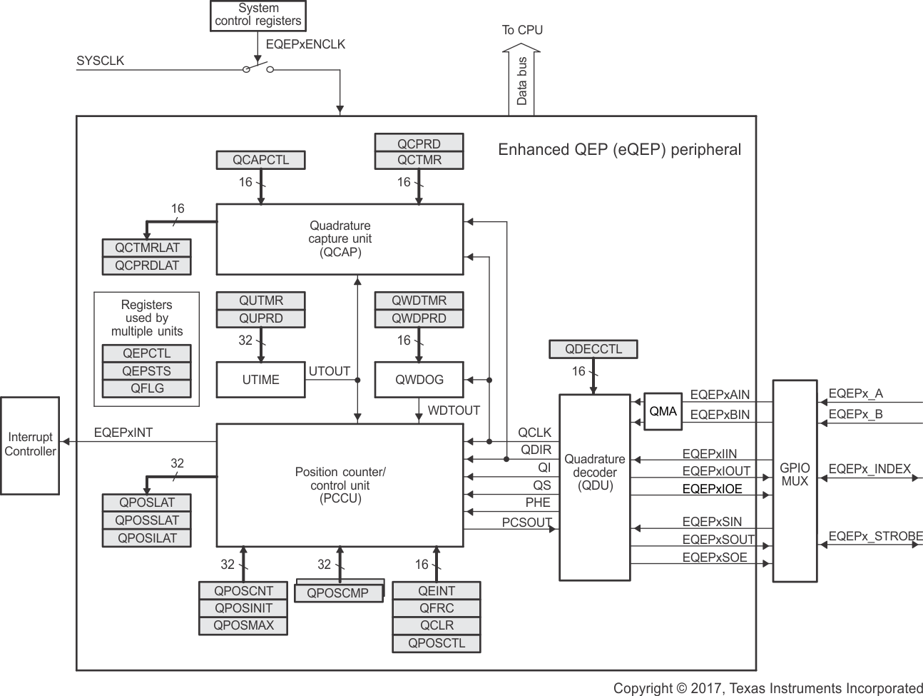
Enhanced Quadrature Encoder Pulse (eQEP)

The eQEP module on this device is Type-2. The eQEP interfaces directly with linear or rotary incremental encoders to obtain position, direction, and speed information from rotating machines used in high-performance motion and position control systems.

The eQEP peripheral contains the following major functional units (see Figure 6-62):

  • Programmable input qualification for each pin (part of the GPIO MUX)
  • Quadrature decoder unit (QDU)
  • Position counter and control unit for position measurement (PCCU)
  • Quadrature edge-capture unit for low-speed measurement (QCAP)
  • Unit time base for speed/frequency measurement (UTIME)
  • Watchdog timer for detecting stalls (QWDOG)
  • Quadrature Mode Adapter (QMA)

F29H859TU-Q1 F29H850TU eQEP
                    Block Diagram Figure 6-62 eQEP Block Diagram