JAJSQA0D december 2011 – december 2020 HD3SS212
PRODUCTION DATA
- 1
- 1 特長
- 2 アプリケーション
- 3 概要
- 4 Revision History
- 5 Pin Configuration and Function
- 6 Specifications
- 7 Parameter Measurement Information
- 8 Detailed Description
- 9 Application and Implementation
- Power Supply Recommendations
- 10Layout
- 11Device and Documentation Support
- 12Mechanical, Packaging, and Orderable Information
9.1.1 AC Coupling Caps
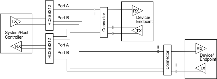
Many interfaces require AC coupling between the transmitter and receiver. The 0402 capacitors are the preferred option to provide AC coupling, and the 0603 size capacitors also work. The 0805 size capacitors and C-packs should be avoided. When placing AC coupling capacitors symmetric placement is best. A capacitor value of 0.1 µF is best and the value should be match for the ± signal pair. The placement should be along the TX pairs on the system board, which are usually routed on the top layer of the board. There are several placement options for the AC coupling capacitors. Because the switch requires a bias voltage, the capacitors must only be placed on one side of the switch. If they are placed on both sides of the switch, a biasing voltage should be provided. A few placement options are shown below. In Figure 9-1, the coupling capacitors are placed between the switch and endpoint. In this situation, the switch is biased by the system/host controller.
 Figure 9-1 AC Coupling Capacitors Between Switch TX and Endpoint TX
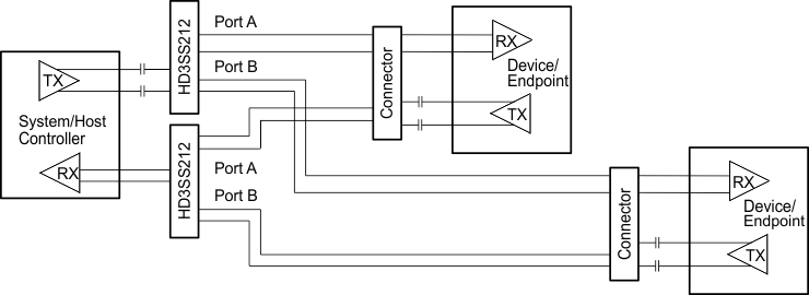
In Figure 9-2, the coupling capacitors are placed on the host transmit pair and endpoint transmit pair. In this situation, the switch on the top is biased by the endpoint and the lower switch is biased by the host controller.
 Figure 9-2 AC Coupling Capacitors on Host TX and Endpoint TX
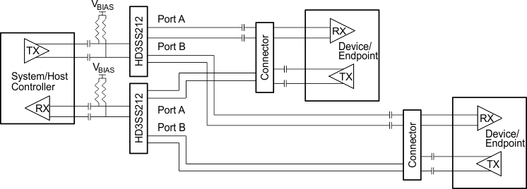
If the common-mode voltage in the system is higher than 2 V, the coupling capacitors are placed on both sides of the switch (shown in Figure 9-3). A biasing voltage of less than 2 V is required in this case.
 Figure 9-3 AC Coupling Capacitors on Both Sides of Switch