JAJSQA0D december 2011 – december 2020 HD3SS212
PRODUCTION DATA
- 1
- 1 特長
- 2 アプリケーション
- 3 概要
- 4 Revision History
- 5 Pin Configuration and Function
- 6 Specifications
- 7 Parameter Measurement Information
- 8 Detailed Description
- 9 Application and Implementation
- Power Supply Recommendations
- 10Layout
- 11Device and Documentation Support
- 12Mechanical, Packaging, and Orderable Information
5 Pin Configuration and Function
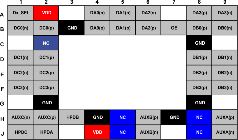
Table 5-1 Pin Functions
| PIN | PIN NAME | I/O | DESCRIPTION |
|---|---|---|---|
| A1 | Dx_SEL | Control I | High Speed Port Selection Control Pins |
| B4 A4 |
DA0(p) DA0(n) |
I/O | Port A, Channel 0, High Speed Positive
Signal Port A, Channel 0, High Speed Negative Signal |
| B5 A5 |
DA1(p) DA1(n) |
I/O | Port A, Channel 1, High Speed Positive
Signal Port A, Channel 1, High Speed Negative Signal |
| B6 A6 |
DA2(p) DA2(n) |
I/O | Port A, Channel 2, High Speed Positive
Signal Port A, Channel 2, High Speed Negative Signal |
| A8 A9 |
DA3(p) DA3(n) |
I/O | Port A, Channel 3, High Speed Positive
Signal Port A, Channel 3, High Speed Negative Signal |
| B8 B9 |
DB0(p) DB0(n) |
I/O | Port B, Channel 0, High Speed Positive
Signal Port B, Channel 0, High Speed Negative Signal |
| D8 D9 |
DB1(p) DB1(n) |
I/O | Port B, Channel 1, High Speed Positive
Signal Port B, Channel 1, High Speed Negative Signal |
| E8 E9 |
DB2(p) DB2(n) |
I/O | Port B, Channel 2, High Speed Positive
Signal Port B, Channel 2, High Speed Negative Signal |
| F8 F9 |
DB3(p) DB3(n) |
I/O | Port B, Channel 3, High Speed Positive
Signal Port B, Channel 3, High Speed Negative Signal |
| B2 B1 |
DC0(p) DC0(n) |
I/O | Port C, Channel 0, High Speed Positive
Signal Port C, Channel 0, High Speed Negative Signal |
| D2 D1 |
DC1(p) DC1(n) |
I/O | Port C, Channel 1, High Speed Positive
Signal Port C, Channel 1, High Speed Negative Signal |
| E2 E1 |
DC2(p) DC2(n) |
I/O | Port C, Channel 2, High Speed Positive
Signal Port C, Channel 2, High Speed Negative Signal |
| F2 F1 |
DC3(p) DC3(n) |
I/O | Port C, Channel 3, High Speed Positive
Signal Port C, Channel 3, High Speed Negative Signal |
| H9 J9 |
AUXA(p) AUXA(n) |
I/O | Port A AUX Positive Signal Port A AUX Negative Signal |
| H6 J6 |
AUXB(p) AUXB(n) |
I/O | Port B AUX Positive Signal Port B AUX Negative Signal |
| H2 H1 |
AUXC(p) AUXC(n) |
I/O | Port C AUX Positive Signal Port C AUX Negative Signal |
| J2, H3, J1 | HPDA/B/C | I/O | Port A/B/C Hot Plug Detect |
| B7 | OE | I | Output Enable |
| A2, J4 | VDD | Supply | 3.3V Positive power supply voltage |
| B3, C8, G2, G8, H4, H7 |
GND | Supply | Negative power supply voltage |
| C2, H5, H8, J5, J8 | NC | Electrically not connected |