JAJSRJ2A September 2000 – January 2024 INA114
PRODUCTION DATA
- 1
- 1 特長
- 2 アプリケーション
- 3 概要
- 4 Pin Configuration and Functions
- 5 Specifications
- 6 Application and Implementation
- 7 Typical Applications
- 8 Device and Documentation Support
- 9 Revision History
- 10Mechanical, Packaging, and Orderable Information
パッケージ・オプション
デバイスごとのパッケージ図は、PDF版データシートをご参照ください。
メカニカル・データ(パッケージ|ピン)
- P|8
- DW|16
サーマルパッド・メカニカル・データ
発注情報
6.1.4 Input Bias Current Return Path
The input impedance of the INA114 is extremely high-approximately 1010Ω. However, a path must be provided for the input bias current of both inputs. This input bias current is typically less than ±1nA, and can be either polarity as a result of cancellation circuitry. High input impedance means that this input bias current changes very little with varying input voltage.
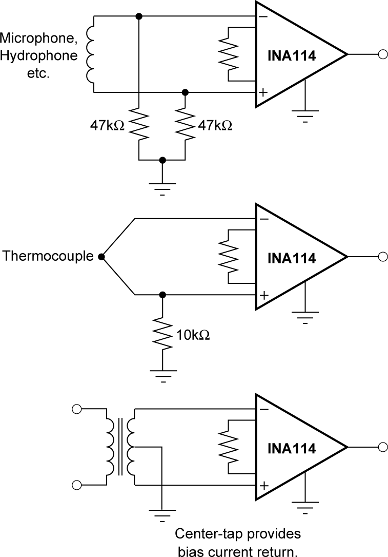
Input circuitry must provide a path for this input bias current if the INA114 is to operate properly. Figure 6-3 shows various provisions for an input bias current path. Without a bias current return path, the inputs float to a potential that exceeds the common-mode range of the INA114 and the input amplifiers saturate. If the differential source resistance is low, the bias current return path can be connected to one input (see thermocouple example in Figure 6-3). With higher source impedance, use two resistors to provide a balanced input, with the possible advantages of lower input offset voltage due to bias current and better common-mode rejection.
 Figure 6-3 Providing an Input Common-Mode
Current Path.