JAJSRJ2A September 2000 – January 2024 INA114
PRODUCTION DATA
- 1
- 1 特長
- 2 アプリケーション
- 3 概要
- 4 Pin Configuration and Functions
- 5 Specifications
- 6 Application and Implementation
- 7 Typical Applications
- 8 Device and Documentation Support
- 9 Revision History
- 10Mechanical, Packaging, and Orderable Information
パッケージ・オプション
デバイスごとのパッケージ図は、PDF版データシートをご参照ください。
メカニカル・データ(パッケージ|ピン)
- P|8
- DW|16
サーマルパッド・メカニカル・データ
発注情報
7 Typical Applications
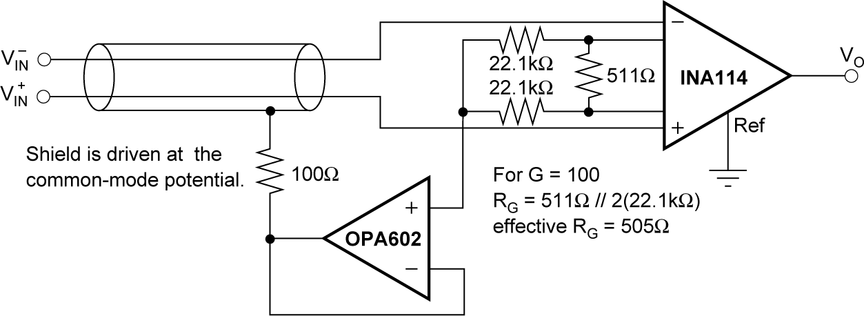
 Figure 7-1 Shield Driver Circuit
 Figure 7-2 RTD Temperature Measurement
Circuit
 Figure 7-3 Thermocouple Amplifier with
Cold Junction Compensation
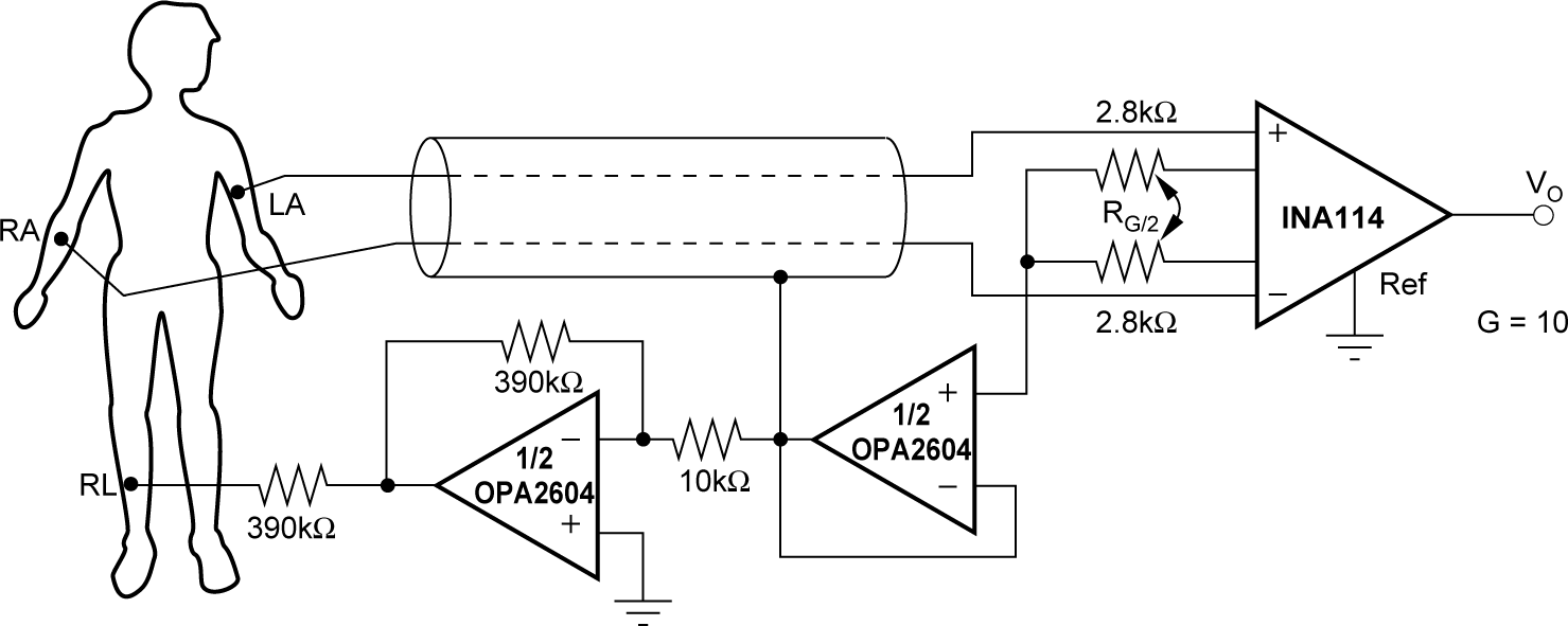
 Figure 7-4 ECG Amplifier with Right-Leg
Drive
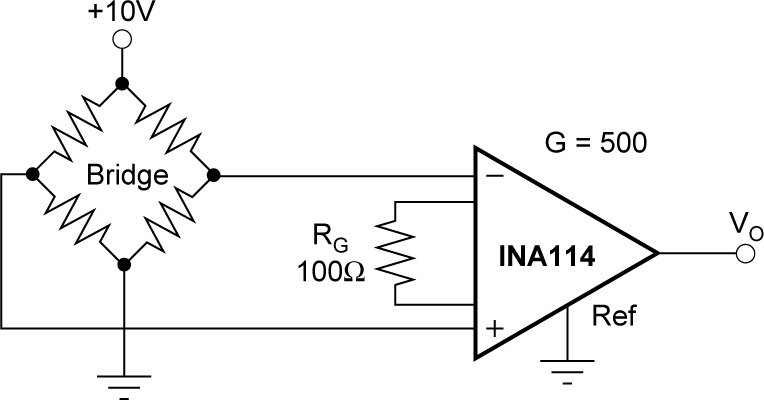
 Figure 7-5 Bridge Transducer
Amplifier
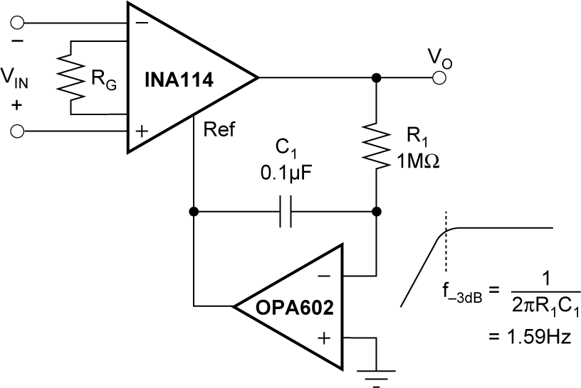
 Figure 7-6 AC-Coupled Instrumentation
Amplifier
 Figure 7-7 Differential
Voltage-to-Current Converter