JAJSUC6B September 2000 – April 2024 INA117
PRODUCTION DATA
- 1
- 1 特長
- 2 アプリケーション
- 3 概要
- 4 Pin Configuration and Functions
- 5 Specifications
- 6 Typical Characteristics
- 7 Application and Implementation
- 8 Device and Documentation Support
- 9 Revision History
- 10Mechanical, Packaging, and Orderable Information
パッケージ・オプション
デバイスごとのパッケージ図は、PDF版データシートをご参照ください。
メカニカル・データ(パッケージ|ピン)
- D|8
- P|8
- LMC|8
サーマルパッド・メカニカル・データ
発注情報
6 Typical Characteristics
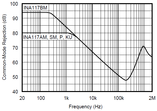 Figure 6-1 Common-mode Rejection vs
Frequency
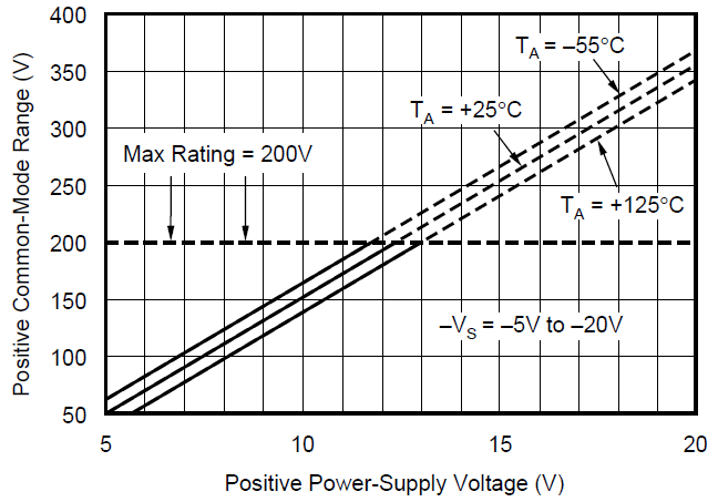 Figure 6-3 Positive Common-mode
Voltage Range vs Positive Power-supply Voltage
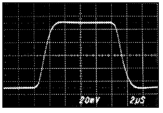 Figure 6-5 Small Signal Step Response
CL = 0pF
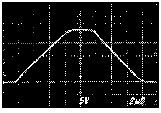 Figure 6-7 Large Signal Step
Response
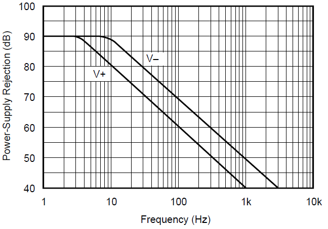 Figure 6-2 Power-supply Rejection vs
Frequency
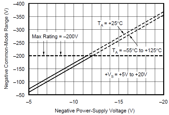 Figure 6-4 Negative Common-mode
Voltage Range vs Negative Power-supply Voltage
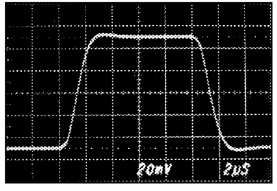 Figure 6-6 Small Signal Step Response
CL = 1000pF