JAJSUC6B September 2000 – April 2024 INA117
PRODUCTION DATA
- 1
- 1 特長
- 2 アプリケーション
- 3 概要
- 4 Pin Configuration and Functions
- 5 Specifications
- 6 Typical Characteristics
- 7 Application and Implementation
- 8 Device and Documentation Support
- 9 Revision History
- 10Mechanical, Packaging, and Orderable Information
パッケージ・オプション
デバイスごとのパッケージ図は、PDF版データシートをご参照ください。
メカニカル・データ(パッケージ|ピン)
- D|8
- P|8
- LMC|8
サーマルパッド・メカニカル・データ
発注情報
7.1.4 Noise Performance
The noise performance of the INA117 is dominated by the internal resistor network. The thermal or Johnson noise of these resistors produces approximately 550nV/√Hz noise. The internal op amp contributes virtually no excess noise at frequencies above 100Hz.
Many applications can be satisfied with less than the full 200kHz bandwidth of the INA117. In these cases, the noise can be reduced with a low-pass filter on the output. The two- pole filter shown in Figure 7-9 limits bandwidth to 1kHz and reduces noise by more than 15:1. Since the INA117 has a 1/f noise corner frequency of approximately 100Hz, a cutoff frequency below 100Hz does not further reduce noise.
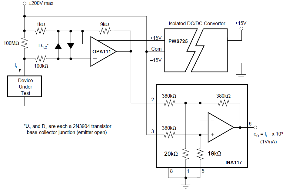
 Figure 7-8 Leakage Current Measurement
Circuit
 Figure 7-9 Output Filter for Noise
Reduction
 Figure 7-10 Summing VX in
Output
 Figure 7-11 Common-mode Voltage
Monitoring
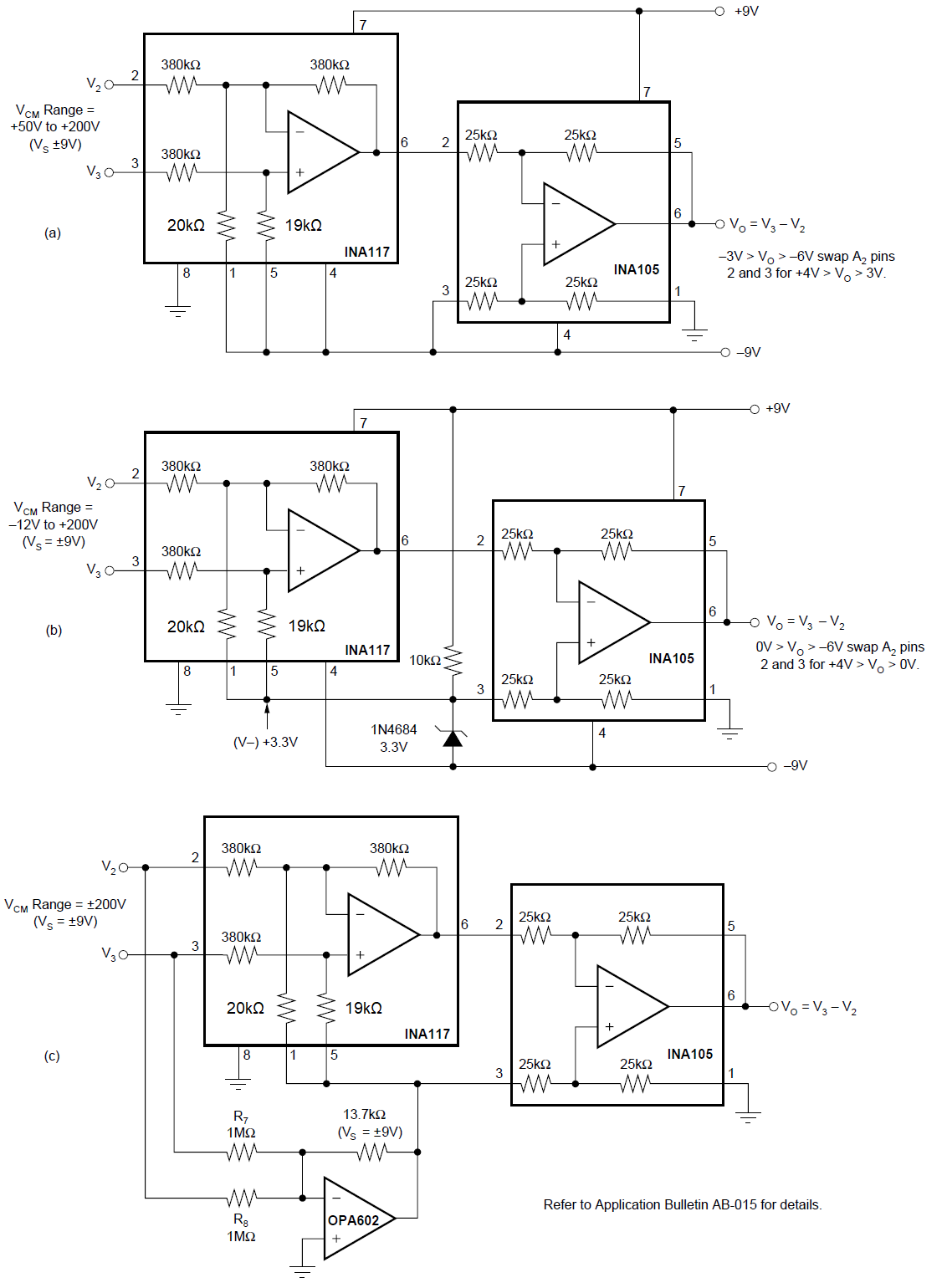
 Figure 7-12 Offsetting or Boosting
Common-mode Voltage Range for Reduced Power-supply Voltage Operation
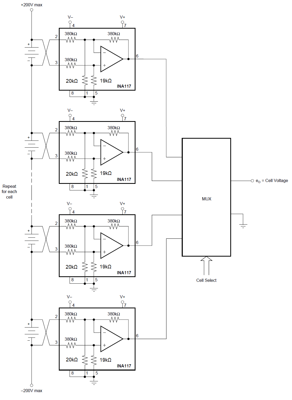
 Figure 7-13 Battery Cell Voltage
Monitor
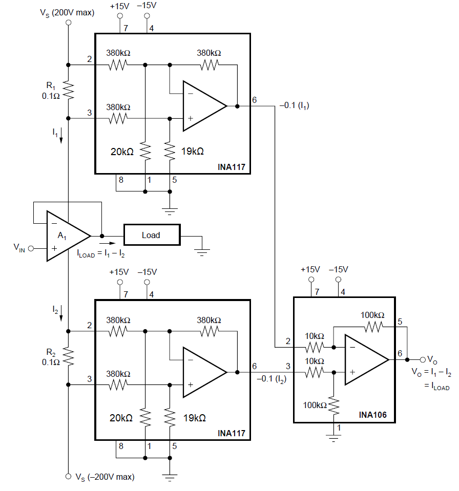
 Figure 7-14 Measuring Amplifier Load
Current
 Figure 7-15 AC-coupled INA117