JAJSH99C September 2000 – September 2022 INA118
PRODUCTION DATA
- 1 特長
- 2 アプリケーション
- 3 概要
- 4 Revision History
- 5 Device Comparison Table
- 6 Pin Configuration and Functions
- 7 Specifications
- 8 Detailed Description
- 9 アプリケーションと実装
- 10Device and Documentation Support
- 11Mechanical, Packaging, and Orderable Information
パッケージ・オプション
メカニカル・データ(パッケージ|ピン)
サーマルパッド・メカニカル・データ
発注情報
9.2.2.4 Input Bias Current Return Path
The input impedance of the INA118 is extremely high at approximately 1010 Ω. However, a path must be provided for the input bias current of both inputs. This input bias current is approximately ±5 nA. High input impedance means that this input bias current changes very little with varying input voltage.
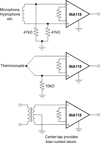
Input circuitry must provide a path for this input bias current for proper operation. Figure 9-3 shows various provisions for an input bias current path. Without a bias current path, the inputs float to a potential which exceeds the common-mode range of the INA118, and the input amplifiers saturates.
If the differential source resistance is low, the bias current return path can be connected to one input (see the thermocouple example in Figure 9-3). With higher source impedance, using two equal resistors provides a balanced input, with the possible advantages of lower input offset voltage due to bias current, and better high-frequency common-mode rejection.
 Figure 9-3 Providing an Input Common-Mode Current Path