SBOS069A October 1997 – December 2024 INA122
PRODUCTION DATA
- 1
- 1 Features
- 2 Applications
- 3 Description
- 4 Pin Configuration and Functions
- 5 Specifications
- 6 Detailed Description
- 7 Application and Implementation
- 8 Device and Documentation Support
- 9 Revision History
- 10Mechanical, Packaging, and Orderable Information
パッケージ・オプション
デバイスごとのパッケージ図は、PDF版データシートをご参照ください。
メカニカル・データ(パッケージ|ピン)
- D|8
- P|8
サーマルパッド・メカニカル・データ
発注情報
5.5 Typical Characteristics
At TA = +25°C and VS = ±5V, unless otherwise noted.
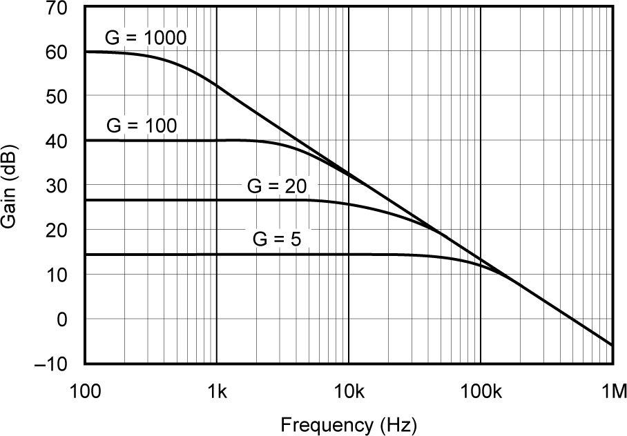 Figure 5-1 Gain vs Frequency
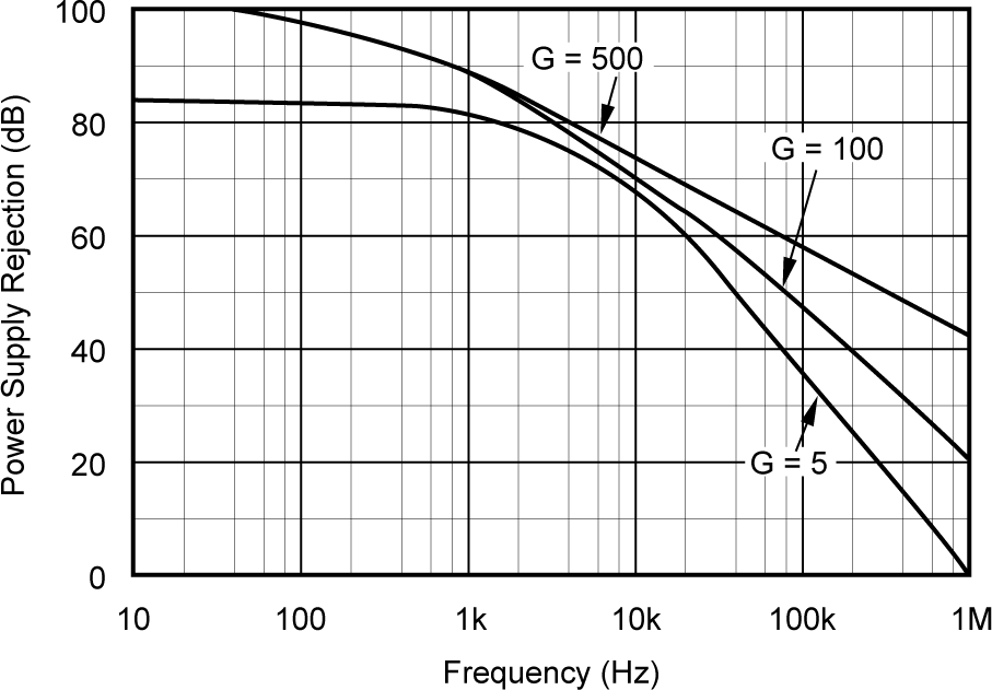 Figure 5-3 Positive Power Supply Rejection vs Frequency
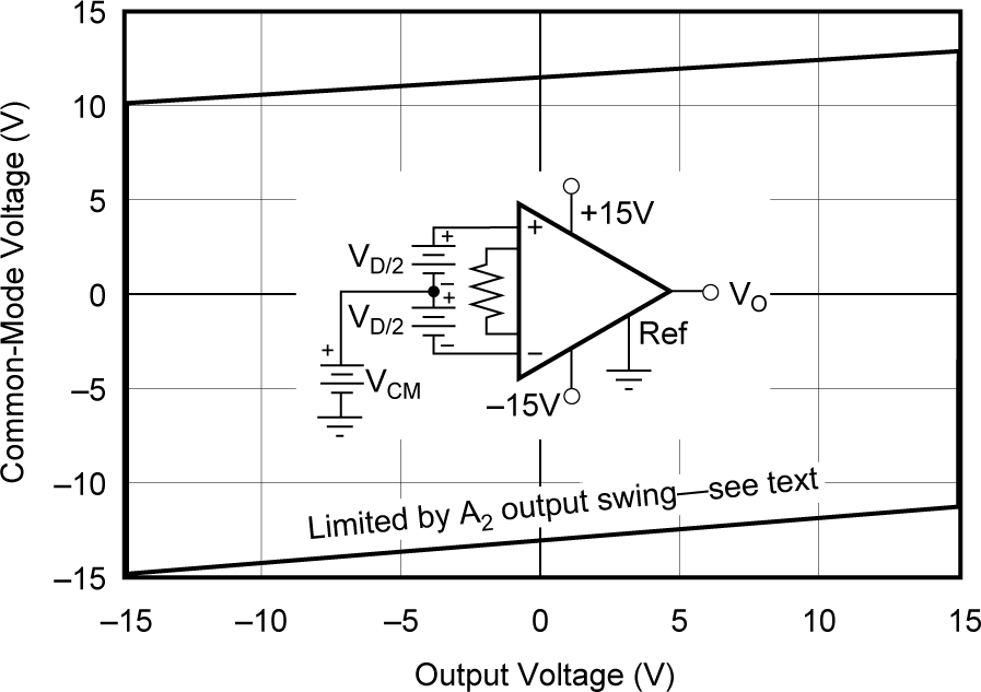 Figure 5-5 Input Common-Mode Range vs Output Voltage, VS = ±15V, G = 5
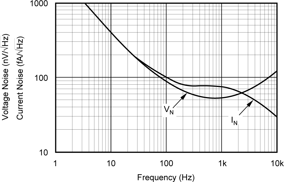 Figure 5-7 Voltage and Current Noise Density vs Frequency
(RTI)
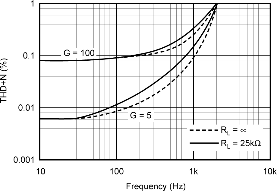 Figure 5-9 Total Harmonic Distortion+Noise vs Frequency
 Figure 5-11 Small-Signal Step Response G = 5
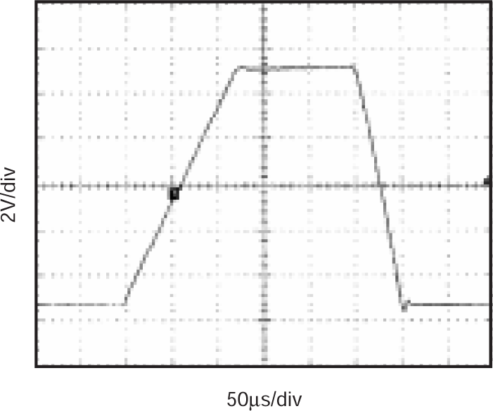 Figure 5-13 Large-Signal Step Response G = 5
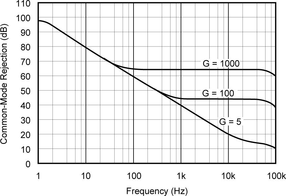 Figure 5-2 Common-Mode Rejection vs Frequency
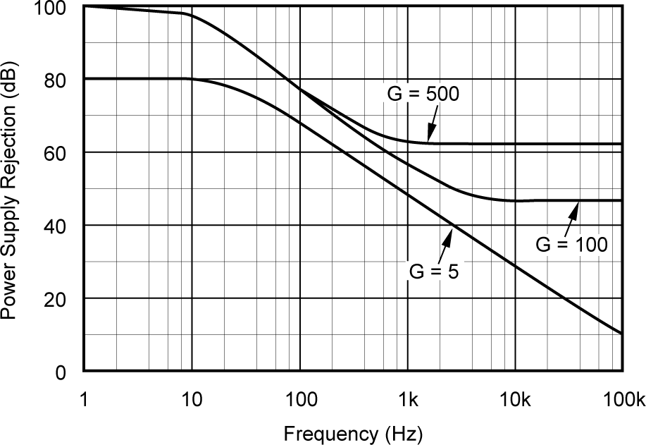 Figure 5-4 Negative Power Supply Rejection vs Frequency
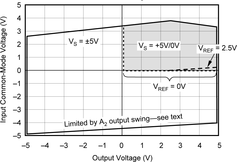 Figure 5-6 Input Common-Mode Voltage vs Output Voltage, VS = ±5V, G = 5
 Figure 5-8 Quiescent Current vs Temperature
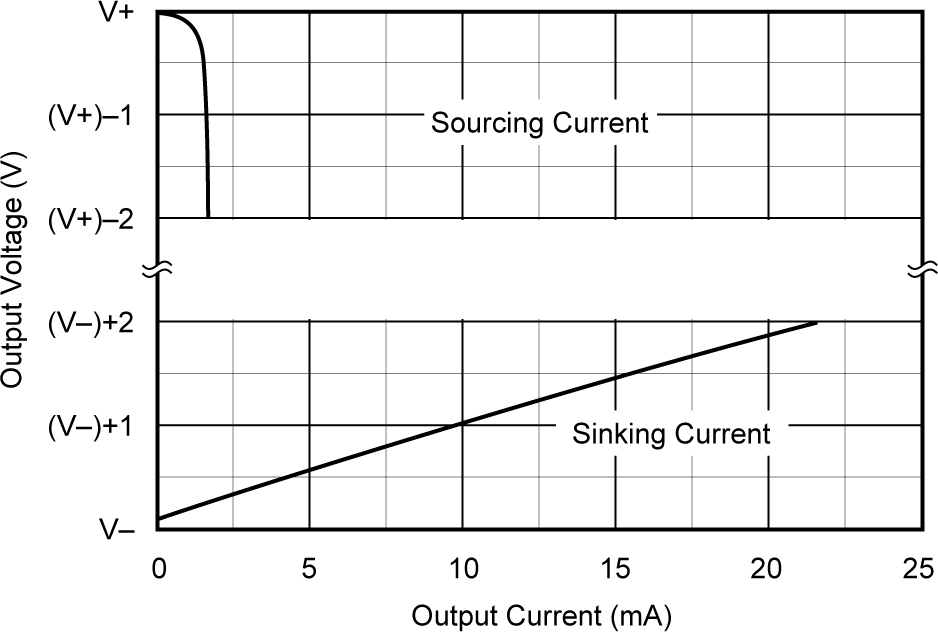 Figure 5-10 Output Voltage Swing vs Output Current
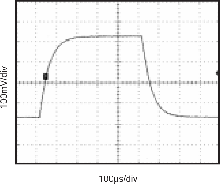 Figure 5-12 Small-Signal Step Response G = 100
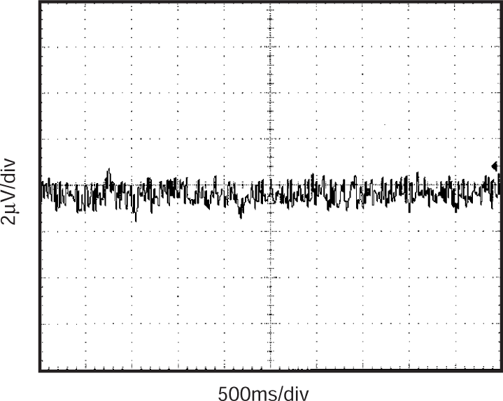 Figure 5-14 Input-Referred Noise Voltage 0.1Hz to 10Hz