-
INA1x9-Q1 Automotive-Grade, High-Side, Current-Output, Current-Shunt Monitor
- 1 Features
- 2 Applications
- 3 Description
- 4 Revision History
- 5 Pin Configuration and Functions
- 6 Specifications
- 7 Detailed Description
-
8 Application and Implementation
- 8.1 Application Information
- 8.2 Typical Applications
- 9 Power Supply Recommendations
- 10Layout
- 11Device and Documentation Support
- 12Mechanical, Packaging, and Orderable Information
- IMPORTANT NOTICE
パッケージ・オプション
デバイスごとのパッケージ図は、PDF版データシートをご参照ください。
メカニカル・データ(パッケージ|ピン)
- PW|8
サーマルパッド・メカニカル・データ
発注情報
INA1x9-Q1 Automotive-Grade, High-Side, Current-Output, Current-Shunt Monitor
1 Features
- Qualified for Automotive Applications
- AEC-Q100 Qualified With the Following Results:
- Device Temperature Grade 1: −40°C to 125°C Ambient Operating Temperature Range
- Device HBM ESD Classification Level 2
- Device CDM ESD Classification Level C6
- Complete Unidirectional High-Side Current Measurement Circuit
- Wide Supply and Common-Mode Ranges
- INA139-Q1: 2.7 V to 40 V
- INA169-Q1: 2.7 V to 60 V
- Independent Supply and Input Common-Mode Voltages
- Single Resistor Gain Set
- Low Quiescent Current (60 μA Typical)
- Wide Temperature Range: –40°C to +125°C
- Package: TSSOP-8
2 Applications
3 Description
The INA139-Q1 and INA169-Q1 (INA1x9-Q1) are high-side, unidirectional, current shunt monitors. Wide input common-mode voltage range, high-speed, low quiescent current, and TSSOP-8 packaging enable use in a variety of applications.
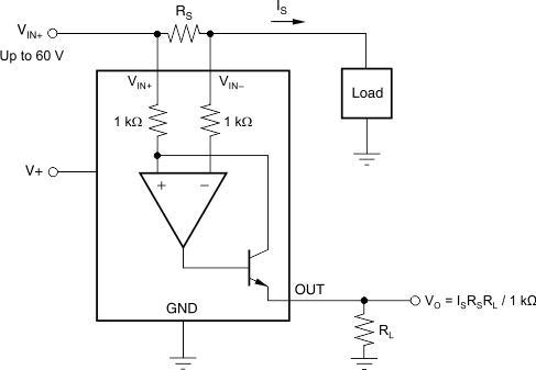
The device converts a differential input voltage to a current output. This current is converted back to a voltage with an external load resistor that sets any gain from 1 to over 100. Although designed for current shunt measurement, the circuit invites creative applications in measurement and level shifting.
Both the INA139-Q1 and INA169-Q1 are available in a TSSOP-8 package, and are specified for the –40°C to +125°C temperature range.
Device Information(1)
| PART NUMBER | PACKAGE | BODY SIZE (NOM) |
|---|---|---|
| INA139-Q1 | TSSOP (8) | 4.40 mm × 3.00 mm |
| INA169-Q1 |
- For all available packages, see the package option addendum at the end of the data sheet.
4 Revision History
Changes from E Revision (May 2011) to F Revision
- Added Device Information, ESD Ratings, Recommended Operating Conditions, and Thermal Information tables, and Feature Description, Application and Implementation, Power Supply Recommendations, Layout, Device and Documentation Support, and Mechanical, Packaging, and Orderable Information sectionsGo
- Added new automotive qualification features bullet, and deleted old bulletGo
- Changed Applications bulletsGo
- Changed text in Description sectionGo
- Changed all figures to show correct device names; added -Q1Go
- Added pin names to all figures and removed all pin numbersGo
- Deleted Ordering Information table; information available in the Package Option Addendum at the end of this data sheetGo
- Deleted lead temperature and thermal resistance from Absolute Maximum Ratings table; see new Thermal Information table for thermal resistance valuesGo
- Changed RθJA valueGo
- Changed VS to V+ throughout data sheet for consistencyGo
- Changed ROUT in Electrical Characteristics table to RL for consistencyGo
- Changed RL from 125 kΩ to 25 kΩ in condition line of Typical Characteristics sectionGo
- Changed VIN to VSENSE in Figure 4Go
- Changed VS to RS when describing shunt resistor in Operation sectionGo
- Changed Figure 9; deleted incorrect pin numbers, and moved embedded table to outside of figureGo
- Changed Figure 10Go
- Changed Figure 14 to show correct pin names, deleted incorrect pin numbers, and added missing division line in output offset equationGo
- Changed Figure 15Go
