JAJSCS8B December 2016 – November 2018 INA1650 , INA1651
PRODUCTION DATA.
- 1 特長
- 2 アプリケーション
- 3 概要
- 4 改訂履歴
- 5 Pin Configuration and Functions
- 6 Specifications
- 7 Detailed Description
-
8 Application and Implementation
- 8.1 Application Information
- 8.2
Typical Applications
- 8.2.1 Line Receiver for Differential Audio Signals in a Split-Supply System
- 8.2.2 Differential Line Receiver for Single-Supply Applications
- 8.2.3 Floating Single-Ended Input Line Receiver for Ground Loop Noise Reduction
- 8.2.4 Floating Single-Ended Input Line Receiver With Differential Outputs
- 8.2.5 TRS Audio Interface in Single-Supply Applications
- 8.2.6 Differential Line Driver With Single-Ended Input
- 9 Power Supply Recommendations
- 10Layout
- 11デバイスおよびドキュメントのサポート
- 12メカニカル、パッケージ、および注文情報
7.3.1 Audio Signal Path
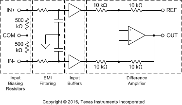
Figure 39 highlights the basic elements present in the audio signal pathway. The primary elements are: input biasing resistors, electromagnetic interference (EMI) filtering, input buffers, and a difference amplifier. The primary role of an audio line receiver is to convert a differential input signal into a single-ended output signal while rejecting noise that is common to both inputs (common-mode noise). The difference amplifier (which consists of an op amp and four matched 10-kΩ resistors) accomplishes this task. The basic transfer function of the circuit is shown in Equation 1:

 Figure 39. INA165x Audio Signal Path (Single Channel Shown)
 The input buffers prevent external resistances (such as those from the PCB, connectors, or cables) from ruining the precise matching of the internal 10-kΩ resistors which would degrade the high common-mode rejection of the difference amplifier. As is typical of many amplifiers, a small bias current flows into or out of the buffer amplifier inputs. This current must flow to a common potential for the buffer to function properly. The input biasing resistors provide an internal pathway for this current to the COM pin. The COM pin can connect to ground in a dual-supply system or the output of the internal supply divider (VMID(OUT)) in single-supply applications. Finally, EMI filtering is added to the input buffers to prevent high-frequency interference signals from propagating through the audio signal pathway.