JAJSCS8B December 2016 – November 2018 INA1650 , INA1651
PRODUCTION DATA.
- 1 特長
- 2 アプリケーション
- 3 概要
- 4 改訂履歴
- 5 Pin Configuration and Functions
- 6 Specifications
- 7 Detailed Description
-
8 Application and Implementation
- 8.1 Application Information
- 8.2
Typical Applications
- 8.2.1 Line Receiver for Differential Audio Signals in a Split-Supply System
- 8.2.2 Differential Line Receiver for Single-Supply Applications
- 8.2.3 Floating Single-Ended Input Line Receiver for Ground Loop Noise Reduction
- 8.2.4 Floating Single-Ended Input Line Receiver With Differential Outputs
- 8.2.5 TRS Audio Interface in Single-Supply Applications
- 8.2.6 Differential Line Driver With Single-Ended Input
- 9 Power Supply Recommendations
- 10Layout
- 11デバイスおよびドキュメントのサポート
- 12メカニカル、パッケージ、および注文情報
8.1.2 Common-Mode Input Impedance
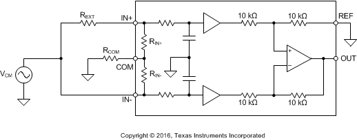
The high CMRR of many line receivers can degrade by impedance mismatches in the system. Figure 42 shows a common-mode noise source (VCM) connected to both inputs of a single channel of the INA165x. An external parasitic resistance (REXT) represents the mismatch in impedances between the common-mode noise source and the inputs of the INA165x. This mismatched impedance may be due to PCB layout, connectors, cabling, passive component tolerances, or the circuit topology. The presence of REXT in series with the IN+ input degrades the overall CMRR of the system because the voltage at IN+ is no longer equal to the voltage at IN–. Therefore, a portion of the common-mode noise converts to a differential signal and passes to the output.
 Figure 42. A Single Channel of the INA165x Shown With Source Impedance Mismatch (REXT) and Optional Resistor (RCOM)
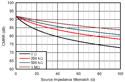
 While the INA165x is significantly more resistant to these effects than typical line receivers, connecting a resistor (RCOM) from the COM pin to the system ground further improves CMRR performance. Figure 43 shows the CMRR of the INA165x (typical CMRR of 92 dB) for increasing source impedance mismatches. If the COM pin is connected directly to ground (RCOM equal to 0 Ω), a 20-Ω source impedance mismatch degrades the CMRR from 92 dB to 83.7 dB. However, if RCOM has a value of 1 MΩ, the CMRR only degrades to 89.6 dB, which is an improvement of approximately 6 dB.
 Figure 43. CMRR vs Source Impedance Mismatch for Different RCOM Values
 RCOM does not need to be a high-precision resistor with a very tight tolerance. Low cost 5% or 1% resistors can be used with no degradation in overall performance. The addition of RCOM does not increase the noise of the audio signal path.
In single-supply systems where AC coupling is used at the inputs of the INA165x, adding RCOM lengthens the start-up time of the circuit. The input AC-coupling capacitors are charged to the midsupply voltage through the RCOM resistor, which may take a substantial amount of time if RCOM has a large value (such as 1 MΩ). Do not use RCOM in these systems if start-up time is a concern. In dual-supply systems with input AC-coupling capacitors, the capacitor voltage does not need to be charged to a midsupply point, since the capacitor voltage settles to ground by default. Therefore, RCOM does not increase start-up time in dual-supply systems.