JAJSCS8B December 2016 – November 2018 INA1650 , INA1651
PRODUCTION DATA.
- 1 特長
- 2 アプリケーション
- 3 概要
- 4 改訂履歴
- 5 Pin Configuration and Functions
- 6 Specifications
- 7 Detailed Description
-
8 Application and Implementation
- 8.1 Application Information
- 8.2
Typical Applications
- 8.2.1 Line Receiver for Differential Audio Signals in a Split-Supply System
- 8.2.2 Differential Line Receiver for Single-Supply Applications
- 8.2.3 Floating Single-Ended Input Line Receiver for Ground Loop Noise Reduction
- 8.2.4 Floating Single-Ended Input Line Receiver With Differential Outputs
- 8.2.5 TRS Audio Interface in Single-Supply Applications
- 8.2.6 Differential Line Driver With Single-Ended Input
- 9 Power Supply Recommendations
- 10Layout
- 11デバイスおよびドキュメントのサポート
- 12メカニカル、パッケージ、および注文情報
8.1.3 Start-Up Time in Single-Supply Applications
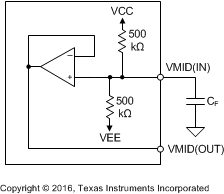
The internal supply divider of the INA165x is constructed using two 500-kΩ resistors connected in series between the VCC and VEE pins. These resistors are matched on-chip to provide a reference voltage that is exactly one half of the power supply voltage. Noise from the power supplies and thermal noise from the resistors degrades the overall audio performance of the INA165x if allowed to enter the signal path. Therefore, TI recommends a filter capacitor (CF) is connected to the VMID(IN) pin, as shown in Figure 44 The CF capacitor forms a low-pass filter with the internal 500-kΩ resistors. Noise above the corner frequency of this filter is passed to ground and is removed from the audio signal path. The corner frequency of the filter is shown in Equation 3:

 Figure 44. Connect a Capacitor (CF) to the VMID(IN) Pin to Reduce Noise from the Voltage Divider
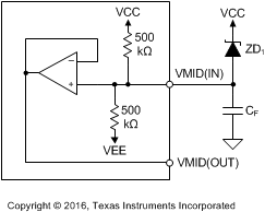
  Figure 45. A Zener Diode (ZD1) Connected to the Positive Supply Can Decrease Start-Up Time
 When power is applied to the INA165x, the filter capacitor (CF) charges through the internal 500-kΩ resistors. If the CF capacitor has a large value, the time required for VMID(OUT) to reach the final midsupply voltage may be extensive. Adding a zener diode from the VMID(IN) pin to the positive power supply (as shown in Figure 45) reduces this time. The zener voltage must be slightly greater than one half of the power supply voltage.
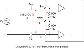
Using large AC-coupling capacitors increases the start-up time of the line receiver circuit in single-supply applications. When power is applied, the AC-coupling capacitors begin to charge to the midsupply voltage applied to the COM pin through a current flowing through the input resistors as shown in Figure 46. The INA165x functions properly when the input common-mode voltage (and the capacitor voltage) is within the specified range. The time required for the input common-mode voltage to reach 98% of the final value is shown in Equation 4:

 Figure 46. AC-Coupling Capacitors Charge to the Midsupply Voltage Through the Input Resistors