JAJSCM5F December 2000 – February 2017 INA139 , INA169
PRODUCTION DATA.
- 1 特長
- 2 アプリケーション
- 3 概要
- 4 改訂履歴
- 5 Pin Configuration and Functions
- 6 Specifications
- 7 Detailed Description
-
8 Application and Implementation
- 8.1 Application Information
- 8.2 Typical Applications
- 9 Power Supply Recommendations
- 10Layout
- 11デバイスおよびドキュメントのサポート
- 12メカニカル、パッケージ、および注文情報
パッケージ・オプション
デバイスごとのパッケージ図は、PDF版データシートをご参照ください。
メカニカル・データ(パッケージ|ピン)
- DBV|5
サーマルパッド・メカニカル・データ
発注情報
8 Application and Implementation
NOTE
Information in the following applications sections is not part of the TI component specification, and TI does not warrant its accuracy or completeness. TI’s customers are responsible for determining suitability of components for their purposes. Customers should validate and test their design implementation to confirm system functionality.
8.1 Application Information
8.1.1 Operation
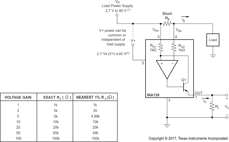
Figure 9 illustrates the basic circuit diagram for both the INA139 and INA169. Load current IS is drawn from supply VS through shunt resistor RS. The voltage drop in shunt resistor VS is forced across RG1 by the internal operational amplifier, causing current to flow into the collector of Q1. The external resistor RL converts the output current to a voltage, VOUT, at the OUT pin.
The transfer function for the INA139 is given by Equation 3:

where
- gm = 1000 µA/V
In the circuit of Figure 9, the input voltage (VIN+ – VIN–) is equal to IS × RS and the output voltage(VOUT) is equal to IO × RL. The transconductance (gm) of the INA139 is 1000 µA/V. The complete transfer function for the current measurement amplifier in this application is given by Equation 4:

The maximum differential input voltage for accurate measurements is 0.5 V, which produces a 500-µA output current. A differential input voltage of up to 2 V will not cause damage. Differential measurements (pins 3 and 4) must be unipolar with a more-positive voltage applied to pin 3. If a more-negative voltage is applied to pin 3, the output current, IO, is zero, but it will not cause damage.
8.2 Typical Applications
The INA139 is designed for current shunt measurement circuits, as shown in Figure 9, but its basic function is useful in a wide range of circuitry. A creative engineer will find many unforeseen uses in measurement and level shifting circuits. A few ideas are illustrated in Figure 14 through Figure 18.
8.2.1 Buffering Output to Drive an ADC
8.2.1.1 Design Requirements
Digitize the output of the INA139 or INA169 devices using a 1-MSPS analog-to-digital converter (ADC).
8.2.1.2 Detailed Design Procedure
8.2.1.2.1 Selecting RS and RL
In Figure 9 the value selected for the shunt resistor ( RS) depends on the application and is a compromise between small-signal accuracy and maximum permissible voltage loss in the measurement line. High values of RS provide better accuracy at lower currents by minimizing the effects of offset, while low values of RS minimize voltage loss in the supply line. For most applications, best performance is attained with an RS value that provides a full-scale shunt voltage of 50 mV to 100 mV; maximum input voltage for accurate measurements is 500 mV.
RL is selected to provide the desired full-scale output voltage. The output impedance of the INA139 and INA169 OUT terminal is very high, which permits using values of RL up to 100 kΩ with excellent accuracy. The input impedance of any additional circuitry at the output must be much higher than the value of RL to avoid degrading accuracy.
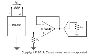
Some analog-to-digital converters (ADCs) have input impedances that significantly affect measurement gain. The input impedance of the ADC can be included as part of the effective RL if the input can be modeled as a resistor to ground. Alternatively, an operational amplifier can be used to buffer the ADC input, as shown in Figure 10. The INA139 and INA169 are current output devices, and have an inherently large output impedance. The output currents from the amplifier are converted to an output voltage through the load resistor (RL) connected from the amplifier output to ground. The ratio of the load resistor value to that of the internal resistor value determines the voltage gain of the system.
In many applications, digitizing the output of the INA139 or INA169 devices is required. This is accomplished by connecting the output of the amplifier to an ADC. It is very common for an ADC to have a dynamic input impedance. If the INA139 or INA169 output is connected directly to an ADC input, the input impedance of the ADC is effectively connected in parallel with the gain setting resistor (RL.) This parallel impedance combination affects the gain of the system and the impact on the gain is difficult to estimate accurately. A simple solution that eliminates the paralleling of impedances, simplifying the gain of the circuit is to place a buffer amplifier (such as the OPA340) between the output of the INA139 or INA169 devices and the input to the ADC.
Figure 10 illustrates this concept. A low-pass filter can be placed between the OPA340 output and the input to the ADC. The filter capacitor is required to provide any instantaneous demand for current required by the input stage of the ADC. The filter resistor is required to isolate the OPA340 output from the filter capacitor to maintain circuit stability. The values for the filter components vary according to the operational amplifier used for the buffer and the particular ADC selected. For more information regarding the design of the low-pass filter, see the 16-bit 1-MSPS Data Acquisition Reference Design for Single-Ended Multiplexed Applications TI Precision Design.
Figure 11 shows the expected results when driving an analog-to-digital converter at 1 MSPS with and without buffering the INA139 or INA169 output. Without the buffer, the high impedance of the INA139 or INA169 reacts with the input capacitance and sample and hold (S/H) capacitance of the analog-to-digital converter and does not allow the S/H to reach the correct final value before the S/H resets and the next conversion starts. Adding the buffer amplifier significantly reduces the output impedance driving the S/H and allows for higher conversion rates than can be achieved without adding the buffer.
8.2.1.3 Application Curve
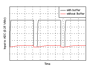 Figure 11. Driving an ADC With and Without a Buffer
8.2.2 Output Filter
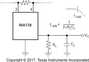 Figure 12. Output Filter
8.2.2.1 Design Requirements
Filter the output of the INA139 or INA169 devices.
8.2.2.2 Detailed Design Procedure
A low-pass filter can be formed at the output of the INA139 or INA169 devices simply by placing a capacitor of the desired value in parallel with the load resistor. First, determine the value of the load resistor required to achieve the desired gain. See the table in Figure 9. Next, determine the capacitor value that results in the desired cutoff frequency according to the equation shown in Figure 12. Figure 13 illustrates various combinations of gain settings (determined by RL) and filter capacitors.
8.2.2.3 Application Curve
 Figure 13. Gain vs Frequency
8.2.3 Offsetting the Output Voltage
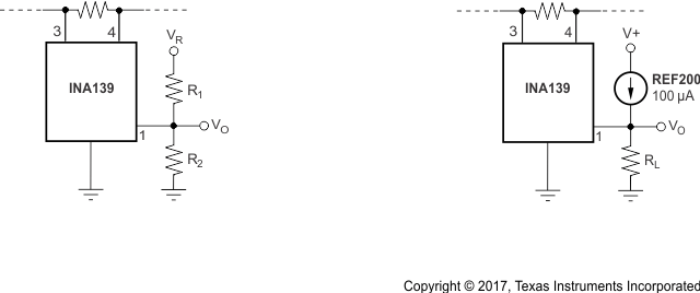
For many applications using only a single power supply, it may be required to level shift the output voltage away from ground when there is no load current flowing in the shunt resistor. Level shifting the output of the INA139 or INA169 devices is easily accomplished by one of two simple methods shown in Figure 14. The method on the left hand side of Figure 14 illustrates a simple voltage divider method. This method is useful for applications that require the output of the INA139 or INA169 devices to remain centered with respect to the power supply at zero load current through the shunt resistor. Using this method the gain is determined by the parallel combination of R1 and R2, while the output offset is determined by the voltage divider ratio R1 and R2. For applications that may require a fixed value of output offset independent of the power supply voltage, TI recommends using the current source method shown on the right hand side of Figure 14 . With this method, a REF200 constant current source is used to generate a constant output offset. Using this method. the gain is determined by RL and the offset is determined by the product of the value of the current source and RL.
8.2.4 Bipolar Current Measurement
The INA139 or INA169 devices can be configured as shown in Figure 15 in applications where measuring current bi-directionally is required. Two INA devices are required connecting their inputs across the shunt resistor as shown in Figure 15. A comparator, such as the TLV3201, is used to detect the polarity of the load current. The magnitude of the load current is monitored across the resistor connected between ground and the connection labeled Output. In this example the 20-kΩ resistor results in a gain of 20 V/V. The 10-kΩ resistors connected in series with the INA139 or INA169 output current are used to develop a voltage across the comparator inputs. Two diodes are required to prevent current flow into the INA139 or INA169 output, as only one device at a time is providing current to the Output connection of the circuit. The circuit functionality is illustrated in Figure 16.
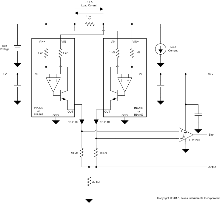 Figure 15. Bipolar Current Measurement
8.2.4.1 Application Curve
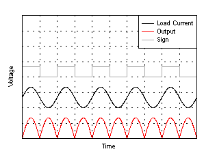 Figure 16. Bipolar Current Measurement Results (Arbitrary Scale)
8.2.5 Bipolar Current Measurement Using a Differential Input of the A/D Converter
The INA139 or INA169 devices can be used with an ADC such as the ADS7870 programmed for differential mode operation. Figure 17 illustrates this configuration. In this configuration, the use of two devices allows for bidirectional current measurement. Depending upon the polarity of the current, one of the devices provides an output voltage while the other output is zero. In this way, the ADC reads the polarity of current directly, without requiring additional circuitry.
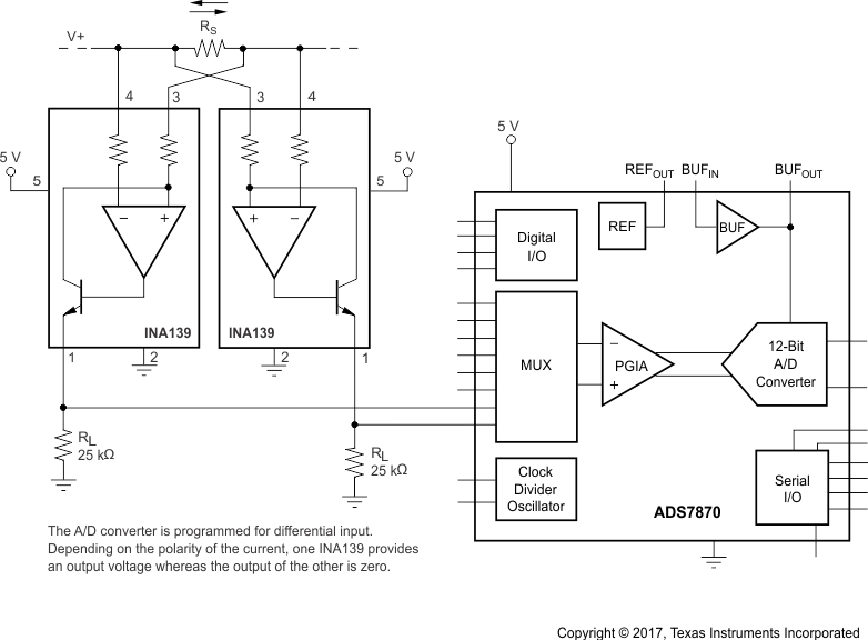 Figure 17. Bipolar Current Measurement Using a Differential Input of the A/D Converter
8.2.6 Multiplexed Measurement Using Logic Signal for Power
Multiple loads can be measured as illustrated in Figure 18. In this configuration, each INA139 or INA169 device is powered by the digital I/O from the ADS7870. Multiplex each device by switching the desired I/O on or off.
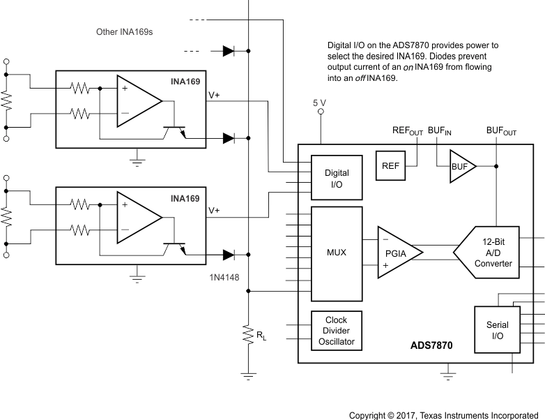 Figure 18. Multiplexed Measurement Using Logic Signal for Power