JAJSHG9A May 2019 – March 2022 INA190-Q1
PRODUCTION DATA
- 1 特長
- 2 アプリケーション
- 3 概要
- 4 Revision History
- 5 Pin Configuration and Functions
- 6 Specifications
- 7 Detailed Description
- 8 Application and Implementation
- 9 Power Supply Recommendations
- 10Layout
- 11Device and Documentation Support
- 12Mechanical, Packaging, and Orderable Information
パッケージ・オプション
メカニカル・データ(パッケージ|ピン)
サーマルパッド・メカニカル・データ
発注情報
7.4.2 Unidirectional Mode
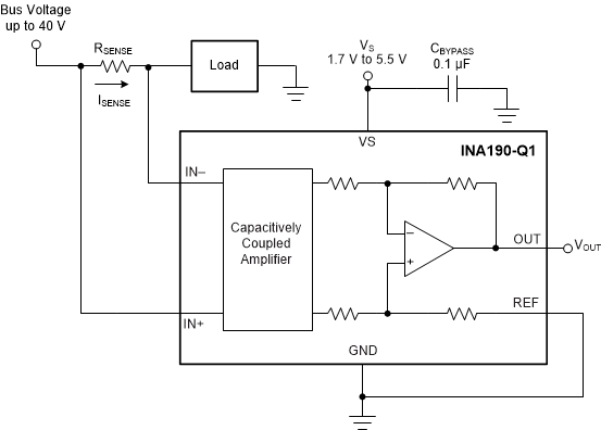
This device can be configured to monitor current flowing in one direction (unidirectional) or in both directions (bidirectional) depending on how the REF pin is connected. Figure 7-2 shows the device operating in unidirectional mode where the output is near ground when no current is flowing. When the current flows from the bus supply to the load, the input voltage from IN+ to IN– increases and causes the output voltage at the OUT pin to increase.
 Figure 7-2 Typical Unidirectional
Application
Figure 7-2 Typical Unidirectional
ApplicationThe linear range of the output stage is limited by how close the output voltage can approach ground under zero input conditions. The zero current output voltage of the INA190-Q1 is very small and for most unidirectional applications the REF pin is simply grounded. However, if the measured current multiplied by the current sense resistor and device gain is less than the zero current output voltage then bias the REF pin to a convenient value above the zero current output voltage to get the output into the linear range of the device. To limit common-mode rejection errors, buffer the reference voltage connected to the REF pin.
A less-frequently used output biasing method is to connect the REF pin to the power-supply voltage, VS. This method results in the output voltage saturating at 40 mV less than the supply voltage when no differential input voltage is present. This method is similar to the output saturated low condition with no differential input voltage when the REF pin is connected to ground. The output voltage in this configuration only responds to currents that develop negative differential input voltage relative to the device IN– pin. Under these conditions, when the negative differential input signal increases, the output voltage moves downward from the saturated supply voltage. The voltage applied to the REF pin must not exceed VS.
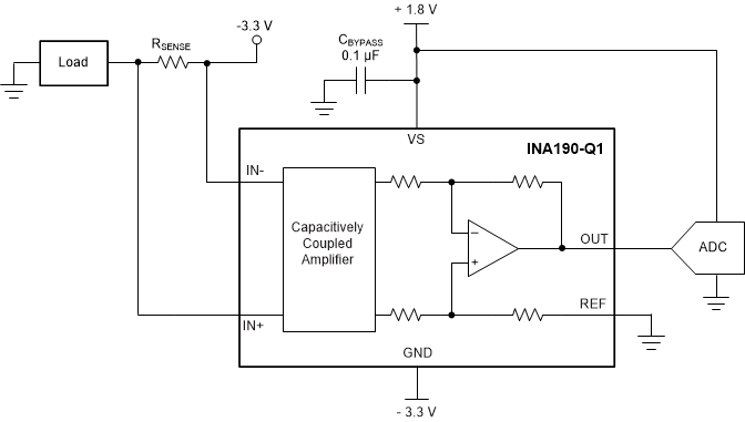
Another use for the REF pin in unidirectional operation is to level shift the output voltage. Figure 7-3 shows an application where the device ground is set to a negative voltage so currents biased to negative supplies, as seen in optical networking cards, can be measured. The GND of the INA190-Q1 can be set to negative voltages, as long as the inputs do not violate the common-mode range specification and the voltage difference between vs. and GND does not exceed 5.5 V. In this example, the output of the INA190-Q1 is fed into a positive-biased ADC. By grounding the REF pin, the voltages at the output will be positive and not damage the ADC. To make sure the output voltage never goes negative, the supply sequencing must be the positive supply first, followed by the negative supply.
 Figure 7-3 Using the
REF Pin to Level-Shift Output Voltage