JAJSF17D March   2018  – November 2019 INA190

PRODUCTION DATA.  

  1. 特長
  2. アプリケーション
  3. 概要
    1.     Device Images
      1.      代表的なアプリケーション
  4. 改訂履歴
  5. Pin Configuration and Functions
    1.     Pin Functions
  6. Specifications
    1. 6.1 Absolute Maximum Ratings
    2. 6.2 ESD Ratings
    3. 6.3 Recommended Operating Conditions
    4. 6.4 Thermal Information
    5. 6.5 Electrical Characteristics
    6. 6.6 Typical Characteristics
  7. Detailed Description
    1. 7.1 Overview
    2. 7.2 Functional Block Diagram
    3. 7.3 Feature Description
      1. 7.3.1 Precision Current Measurement
      2. 7.3.2 Low Input Bias Current
      3. 7.3.3 Low Quiescent Current With Output Enable
      4. 7.3.4 Bidirectional Current Monitoring
      5. 7.3.5 High-Side and Low-Side Current Sensing
      6. 7.3.6 High Common-Mode Rejection
      7. 7.3.7 Rail-to-Rail Output Swing
    4. 7.4 Device Functional Modes
      1. 7.4.1 Normal Operation
      2. 7.4.2 Unidirectional Mode
      3. 7.4.3 Bidirectional Mode
      4. 7.4.4 Input Differential Overload
      5. 7.4.5 Shutdown
  8. Application and Implementation
    1. 8.1 Application Information
      1. 8.1.1 Basic Connections
      2. 8.1.2 RSENSE and Device Gain Selection
      3. 8.1.3 Signal Conditioning
      4. 8.1.4 Common-Mode Voltage Transients
    2. 8.2 Typical Applications
      1. 8.2.1 Design Requirements
      2. 8.2.2 Detailed Design Procedure
      3. 8.2.3 Application Curve
  9. Power Supply Recommendations
  10. 10Layout
    1. 10.1 Layout Guidelines
    2. 10.2 Layout Examples
  11. 11デバイスおよびドキュメントのサポート
    1. 11.1 ドキュメントのサポート
      1. 11.1.1 関連資料
    2. 11.2 ドキュメントの更新通知を受け取る方法
    3. 11.3 サポート・リソース
    4. 11.4 商標
    5. 11.5 静電気放電に関する注意事項
    6. 11.6 Glossary
  12. 12メカニカル、パッケージ、および注文情報

パッケージ・オプション

メカニカル・データ(パッケージ|ピン)
サーマルパッド・メカニカル・データ
発注情報

Typical Characteristics

at TA = 25°C, VS = 1.8 V, VIN+ = 12 V, VREF = VS / 2, VENABLE = VS, and for all gain options (unless otherwise noted)
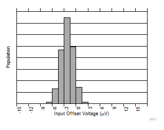
INA190 D001_SBOS863.gif
Figure 1. Input Offset Voltage Production Distribution
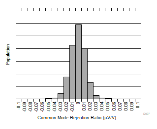
INA190 D007_SBOS863.gif
Figure 3. Common-Mode Rejection Production Distribution
INA190 D013_SBOS863.gif
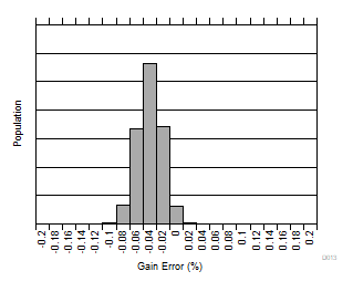
A1 devices
Figure 5. Gain Error Production Distribution
INA190 D017_SBOS863.gif
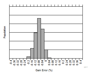
A5 devices
Figure 7. Gain Error Production Distribution
INA190 D019_SBOS863.gif
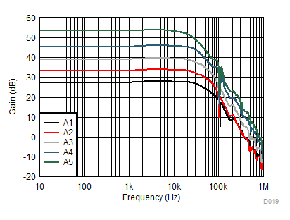
VS = 5 V
Figure 9. Gain vs Frequency
INA190 D021_SBOS863.gif
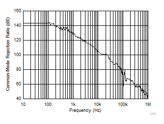
A3 devices
Figure 11. Common-Mode Rejection Ratio vs Frequency
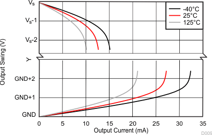
INA190 D009_SBOS863.gif
VS = 5.0 V
Figure 13. Output Voltage Swing vs Output Current
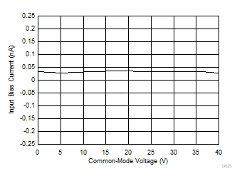
INA190 D025_SBOS863.gif
VENABLE = 0 V
Figure 15. Input Bias Current vs Common-Mode Voltage (Shutdown)
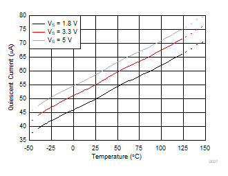
INA190 D027_SBOS863.gif
Figure 17. Quiescent Current vs Temperature (Enabled)
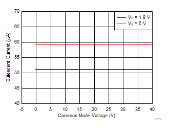
INA190 D029_SBOS863.gif
VS = 5.0 V
Figure 19. Quiescent Current vs Common Mode Voltage
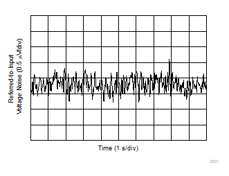
INA190 D031_SBOS863.gif
A3 devices
Figure 21. 0.1-Hz to 10-Hz Voltage Noise (Referred-To-Input)
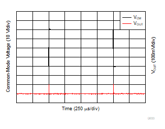
INA190 D033_SBOS863.gif
A3 devices
Figure 23. Common-Mode Voltage Transient Response
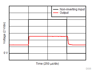
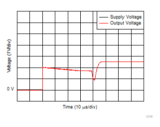
INA190 D035_SBOS863.gif
VS = 5.0 V, A3 devices
Figure 25. Noninverting Differential Input Overload
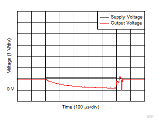
INA190 D037_SBOS863.gif
VS = 5.0 V, A3 devices
Figure 27. Brownout Recovery
INA190 D039_SBOS863.gif
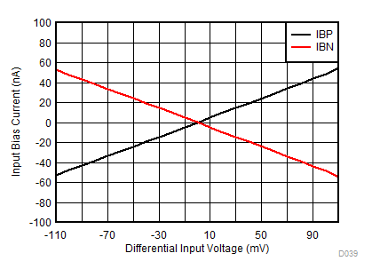
VS = 5.0 V, VREF = 2.5 V, A1 devices
Figure 29. IB+ and IB– vs Differential Input Voltage
INA190 D040_SBOS863.gif
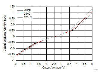
VS = 5.0 V, VENABLE = 0 V, VREF = 2.5 V
Figure 31. Output Leakage vs Output Voltage
(A1, A2, and A3 Devices)
INA190 D050_SBOS863.gif
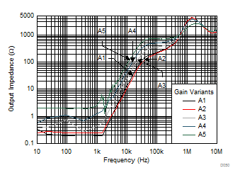
VS = 5.0 V, VCM = 0 V
Figure 33. Output Impedance vs Frequency
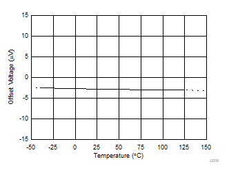
INA190 D006_SBOS863.gif
Figure 2. Offset Voltage vs Temperature
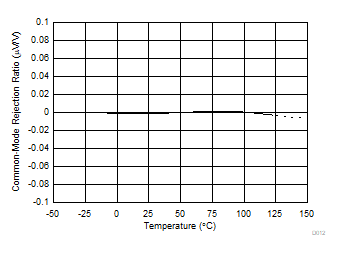
INA190 D012_SBOS863.gif
Figure 4. Common-Mode Rejection Ratio vs Temperature
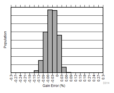
INA190 D014_SBOS863.gif
A2, A3, and A4 devices
Figure 6. Gain Error Production Distribution
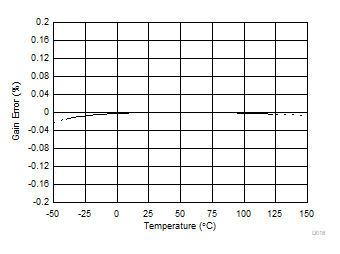
INA190 D018_SBOS863.gif
Figure 8. Gain Error vs Temperature
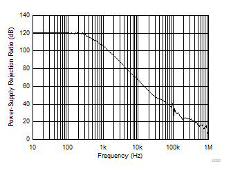
INA190 D020_SBOS863.gif
VS = 5 V
Figure 10. Power-Supply Rejection Ratio vs Frequency
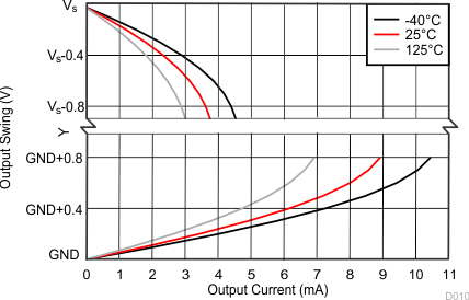
INA190 D010_SBOS863.gif
VS = 1.8 V
Figure 12. Output Voltage Swing vs Output Current
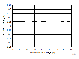
INA190 D024_SBOS863.gif
VS = 5.0 V
Figure 14. Input Bias Current vs Common-Mode Voltage
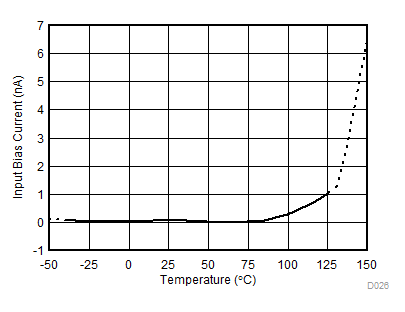
INA190 D026_SBOS863.gif
Figure 16. Input Bias Current vs Temperature
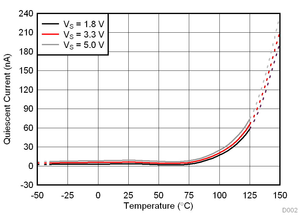
INA190 D002_SBOS863.gif
VENABLE = 0 V
Figure 18. Quiescent Current vs Temperature (Disabled)
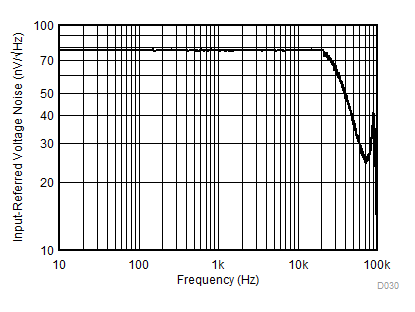
INA190 D030_SBOS863.gif
A3 devices
Figure 20. Input-Referred Voltage Noise vs Frequency
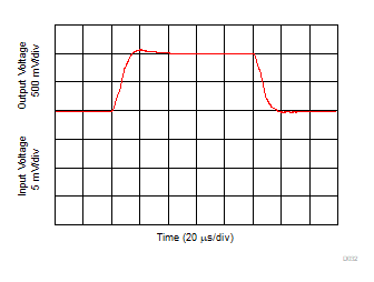
INA190 D032_SBOS863.gif
VS = 5.0 V, A3 devices
Figure 22. Step Response (10-mVPP Input Step)
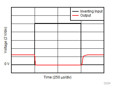
INA190 D034_SBOS863.gif
A3 devices
Figure 24. Inverting Differential Input Overload
INA190 D036_SBOS863.gif
VS = 5.0 V, A3 devices
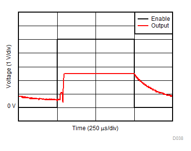
Figure 26. Start-Up Response
INA190 D038_SBOS863.gif
VS = 5.0 V, A3 devices
Figure 28. Enable and Disable Response
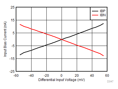
INA190 D047_SBOS863.gif
VS = 5.0 V, VREF = 2.5 V, A2, A3, A4, A5 devices
Figure 30. IB+ and IB– vs Differential Input Voltage
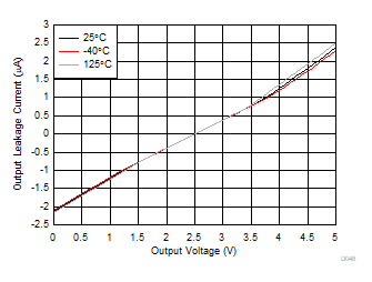
INA190 D048_SBOS863.gif
VS = 5.0 V, VENABLE = 0 V, VREF = 2.5 V
Figure 32. Output Leakage vs Output Voltage
(A4 and A5 Devices)