JAJSCM1A December 2010 – April 2016 INA203-Q1
PRODUCTION DATA.
- 1 特長
- 2 アプリケーション
- 3 概要
- 4 改訂履歴
- 5 Device Comparison Table
- 6 Pin Configuration and Functions
-
7 Specifications
- 7.1 Absolute Maximum Ratings
- 7.2 ESD Ratings
- 7.3 Recommended Operating Conditions
- 7.4 Thermal Information
- 7.5 Electrical Characteristics: Current-Shunt Monitor
- 7.6 Electrical Characteristics: Comparator
- 7.7 Electrical Characteristics: Reference
- 7.8 Electrical Characteristics: General
- 7.9 Typical Characteristics
- 8 Detailed Description
- 9 Application and Implementation
- 10Power Supply Recommendations
- 11Layout
- 12デバイスおよびドキュメントのサポート
- 13メカニカル、パッケージ、および注文情報
9 Application and Implementation
NOTE
Information in the following applications sections is not part of the TI component specification, and TI does not warrant its accuracy or completeness. TI’s customers are responsible for determining suitability of components for their purposes. Customers should validate and test their design implementation to confirm system functionality.
9.1 Application Information
The INA203-Q1 device is designed to enable easy configuration for detecting overcurrent conditions and current monitoring in an application. This device is also incorporate two open-drain comparators with internal 0.6-V references. The comparator references can be overridden by external inputs. Comparator 1 includes a latching capability, and Comparator 2 has a user-programmable delay. The INA203-Q1 also provides a 1.2-V reference output. This device can also be paired with minimum additional devices to create more sophisticated monitoring functional blocks.
9.1.1 Basic Connections
Figure 30 shows the basic connections of the INA203-Q1. Connect the input pins, VIN+ and VIN–, as closely as possible to the shunt resistor to minimize any resistance in series with the shunt resistance.
Power-supply bypass capacitors are required for stability. Applications with noisy or high-impedance power supplies may require additional decoupling capacitors to reject power-supply noise. Connect bypass capacitors close to the device pins.
 Figure 30. INA203-Q1 Basic Connection
9.1.2 Selecting RSHUNT
The value chosen for the shunt resistor, RSHUNT, depends on the application and is a compromise between small-signal accuracy and maximum permissible voltage loss in the measurement line. High values of RSHUNT provide better accuracy at lower currents by minimizing the effects of offset, while low values of RSHUNT minimize voltage loss in the supply line. For most applications, best performance is attained with an RSHUNT value that provides a full-scale shunt voltage range of 50 mV to 100 mV. Maximum input voltage for accurate measurements is (VSHUNT – 0.25)/Gain.
9.1.3 Input Filtering
An obvious and straightforward location for filtering is at the output of the INA203-Q1 series; however, this location negates the advantage of the low output impedance of the internal buffer. The only other option for filtering is at the input pins of the INA203-Q1, which is complicated by the internal 5 kΩ + 30% input impedance; this configuration is illustrated in Figure 31. Using the lowest possible resistor values minimizes both the initial shift in gain and effects of tolerance. Equation 2 gives the effect on initial gain:

To calculate the total effect on gain error, replace the 5-kΩ term with 5 kΩ – 30%, (or 3.5 kΩ) or 5 kΩ + 30% (or 6.5 kΩ). The tolerance extremes of RFILT can also be inserted into the equation. If a pair of 100-Ω 1% resistors are used on the inputs, then the initial gain error will be 1.96%. Worst-case tolerance conditions will always occur at the lower excursion of the internal 5-kΩ resistor (3.5 kΩ), and the higher excursion of RFILT + 3% in this case.
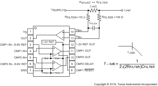 Figure 31. Input Filter
NOTE
The specified accuracy of the INA203-Q1 must then be combined in addition to these tolerances. While this discussion treated accuracy worst-case conditions by combining the extremes of the resistor values, it is appropriate to use geometric-mean or root-sum-square calculations to total the effects of accuracy variations.
9.1.4 Accuracy Variations as a Result of VSENSE and Common-Mode Voltage
The accuracy of the INA203-Q1 current-shunt monitors is a function of two main variables: VSENSE (VIN+ – VIN–) and common-mode voltage, VCM, relative to the supply voltage, VS. VCM is expressed as (VIN+ + VIN–)/2; however, in practice, VCM is seen as the voltage at VIN+ because the voltage drop across VSENSE is usually small.
This section addresses the accuracy of these specific operating regions:
- Normal Case 1: VSENSE ≥ 20 mV, VCM ≥ VS
- Normal Case 2: VSENSE ≥ 20 mV, VCM < VS
- Low VSENSE Case 1: VSENSE < 20 mV, –16 V ≤ VCM < 0
- Low VSENSE Case 2: VSENSE < 20 mV, 0 V ≤ VCM ≤ VS
- Low VSENSE Case 3: VSENSE < 20 mV, VS < VCM ≤ 80 V
9.1.4.1 Normal Case 1: VSENSE ≥ 20 mV, VCM ≥ VS
This region of operation provides the highest accuracy. Here, the input offset voltage is characterized and measured using a two-step method. First, the gain is determined by Equation 3.

where
- VOUT1 = output voltage with VSENSE = 100 mV
- VOUT2 = output voltage with VSENSE = 20 mV
Then the offset voltage is measured at VSENSE = 100 mV and referred to the input (RTI) of the current shunt monitor, as shown in Equation 4.

In the Typical Characteristics section, the Output Error vs Common-Mode Voltage curve (Figure 7) shows the highest accuracy for this region of operation. In this plot, VS = 12 V; for VCM ≥ 12 V, the output error is at its minimum. This case is also used to create the VSENSE ≥ 20 mV output specifications in the Electrical Characteristics table.
9.1.4.2 Normal Case 2: VSENSE ≥ 20 mV, VCM < VS
This region of operation has slightly less accuracy than Normal Case 1 as a result of the common-mode operating area in which the part functions, as seen in the Output Error vs Common-Mode Voltage curve (Figure 7). As noted, for this graph VS = 12 V; for VCM < 12 V, the output error increases as VCM becomes less than 12 V, with a typical maximum error of 0.005% at the most negative VCM = –16 V.
9.1.4.3 Low VSENSE Case 1:
VSENSE < 20 mV, –16 V ≤ VCM < 0; and
Low VSENSE Case 3:
VSENSE < 20 mV, VS < VCM ≤ 80 V
Although the INA203-Q1 is not designed for accurate operation in either of these regions, some applications are exposed to these conditions; for example, when monitoring power supplies that are switched on and off while VS is still applied to the INA203-Q1. It is important to know what the behavior of the devices will be in these regions.
As VSENSE approaches 0 mV, in these VCM regions, the device output accuracy degrades. A larger-than-normal offset can appear at the current shunt monitor output with a typical maximum value of VOUT = 300 mV for VSENSE = 0 mV. As VSENSE approaches 20 mV, VOUT returns to the expected output value with accuracy as specified in the Electrical Characteristics. Figure 32 illustrates this effect (Gain = 100).
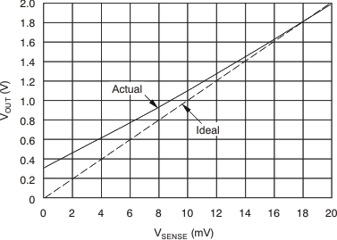
| Data taken from INA205, a device of INA20x family with Gain = 100 | ||
9.1.4.4 Low VSENSE Case 2: VSENSE < 20 mV, 0 V ≤ VCM ≤ VS
This region of operation is the least accurate for the INA203-Q1. To achieve the wide input common-mode voltage range, this device uses two operational amplifiers (Opamp) front ends in parallel. One Opamp front end operates in the positive input common-mode voltage range, and the other in the negative input region. For this case, neither of these two internal amplifiers dominate and overall loop gain is very low. Within this region, VOUT approaches voltages close to linear operation levels for Normal Case 2. This deviation from linear operation becomes greatest the closer VSENSE approaches 0 V. Within this region, as VSENSE approaches 20 mV, device operation is closer to that described by Normal Case 2. Figure 33 illustrates this behavior. The VOUT maximum peak for this case is tested by maintaining a constant VS, setting VSENSE = 0 mV, and sweeping VCM from 0 V to VS. The exact VCM at which VOUT peaks during this test varies from part to part, but the VOUT maximum peak is tested to be less than the specified VOUT Tested Limit.
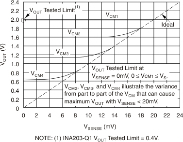
| Data taken from INA205, a device of INA20x family with Gain = 100 | ||
9.1.5 Transient Protection
The –16 V to +80 V common-mode range of the INA203-Q1 is ideal for withstanding automotive fault conditions ranging from 12-V battery reversal up to 80-V transients, since no additional protective components are needed up to those levels. In the event that the INA203-Q1 is exposed to transients on the inputs in excess of their ratings, then external transient absorption with semiconductor transient absorbers (zeners or Transzorbs) are necessary. Use of metal oxide varistors (MOVs) or video disk recorders (VDRs) is not recommended except when they are used in addition to a semiconductor transient absorber. Select the transient absorber such that it will never allow the INA203-Q1 to be exposed to transients greater than 80 V (that is, allow for transient absorber tolerance, as well as additional voltage because of transient absorber dynamic impedance). Despite the use of internal zener-type ESD protection, the INA203-Q1 does not lend itself to using external resistors in series with the inputs because the internal gain resistors can vary up to ±30% but are closely matched. (If gain accuracy is not important, then resistors can be added in series with the INA203-Q1 inputs with two equal resistors on each input.)
9.2 Typical Applications
9.2.1 Polyswitch Warning and Fault Detection Circuit
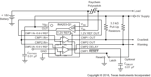 Figure 34. Polyswitch Warning and Fault Detection Circuit Schematic
9.2.1.1 Design Requirements
The device measures current through a resistive shunt with current flowing in one direction, thus enabling detection of an overlimit or warning event only when the differential input voltage exceeds the corresponding threshold limits. When the current reaches the warning limit of 0.6 V, the output of CMP2 will transition high indicating a warning condition. When the current further increases to or past the overlimit limit of 1.2 V, the output of CMP1 will transition high indicating an overlimit condition. Optional CDELAY can be sized to add delay to CMP2.
9.2.1.2 Detailed Design Procedure
Figure 34 shows the basic connections of the device. The input terminals, VIN+ and VIN–, should be connected as close as possible to the current-sensing resistor or polymeric switch to minimize any resistance in series with the shunt resistance. Additional resistance between the current-sensing resistor and input terminals can result in errors in the measurement. When input current flows through this external input resistance, the voltage developed across the shunt resistor can differ from the voltage reaching the input terminals.
9.2.1.3 Application Curves
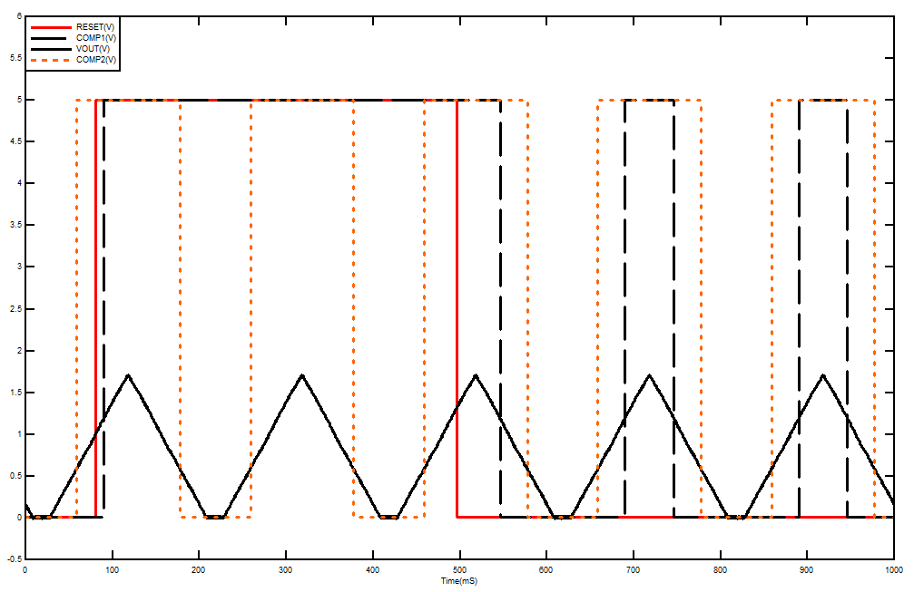 Figure 35. Polyswitch Warning and Fault Detection Circuit Response
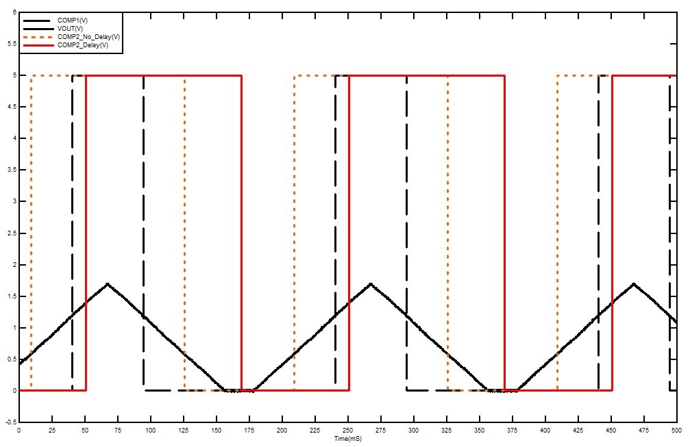 Figure 36. Polyswitch Warning and Fault Detection Circuit With Delay Response
9.2.2 Lead-Acid Battery Protection Circuit
See Figure 37 for a protection scheme using INA203-Q1 for a lead-acid battery application.
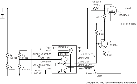 Figure 37. Lead-Acid Battery Protection Circuit Schematic