JAJSCM1A December 2010 – April 2016 INA203-Q1
PRODUCTION DATA.
- 1 特長
- 2 アプリケーション
- 3 概要
- 4 改訂履歴
- 5 Device Comparison Table
- 6 Pin Configuration and Functions
-
7 Specifications
- 7.1 Absolute Maximum Ratings
- 7.2 ESD Ratings
- 7.3 Recommended Operating Conditions
- 7.4 Thermal Information
- 7.5 Electrical Characteristics: Current-Shunt Monitor
- 7.6 Electrical Characteristics: Comparator
- 7.7 Electrical Characteristics: Reference
- 7.8 Electrical Characteristics: General
- 7.9 Typical Characteristics
- 8 Detailed Description
- 9 Application and Implementation
- 10Power Supply Recommendations
- 11Layout
- 12デバイスおよびドキュメントのサポート
- 13メカニカル、パッケージ、および注文情報
8 Detailed Description
8.1 Overview
The INA203-Q1 device is a unidirectional voltage output current-sense amplifier with dual comparators and voltage reference. The INA203-Q1 operates over a wide range of common-mode voltage (–16 V to +80 V) and incorporates two open-drain comparators with internal 0.6-V references. Comparator 1 includes a latching capability, and Comparator 2 has a user-programmable delay. The device also incorporates a 1.2-V reference output.
8.3 Feature Description
8.3.1 Comparator
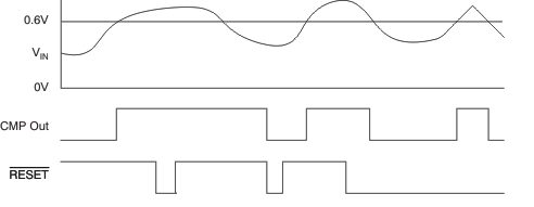
The INA203-Q1 incorporates two open-drain comparators. These comparators typically have 2 mV of offset and a 1.3-μs (typical) response time. The output of Comparator 1 latches and is reset through the CMP1 RESET pin, as shown in Figure 26.
The INA203-Q1 device includes additional features for comparator functions. The comparator reference voltage of both Comparator 1 and Comparator 2 can be overridden by external inputs for increased design flexibility. Comparator 2 has a programmable delay.
 Figure 26. Comparator Latching Capability
8.3.2 Comparator Delay
The Comparator 2 programmable delay is controlled by a capacitor connected to the CMP2 Delay Pin; see Figure 30. The capacitor value (in μF) is selected by using Equation 1:

A simplified version of the delay circuit for Comparator 2 is shown in Figure 27. The delay comparator consists of two comparator stages with the delay between them.
NOTE
I1 and I2 cannot be turned on simultaneously; I1 corresponds to a U1 low output and I2 corresponds to a U1 high output.
Using an initial assumption that the U1 output is low, I1 is on, then U2 +IN is zero. If U1 goes high, I2 supplies 120 nA to CDELAY. The voltage at U2 +IN begins to ramp toward a 0.6-V threshold. When the voltage crosses this threshold, the U2 output goes high while the voltage at U2 +IN continues to ramp up to a maximum of 1.2 V when given sufficient time (twice the value of the delay specified for CDELAY). This entire sequence is reversed when the comparator outputs go low, so that returning to low exhibits the same delay.
 Figure 27. Simplified Model of The Comparator 2 Delay Circuit
It is important to note the behavior of the Comparator 2 when the events at the inputs occur more rapidly than the set delay timeout. For example, when the U1 output goes high (turning on I2), but returns low (turning I1 back on) prior to reaching the 0.6 V transition for U2. The voltage at U2 +IN ramps back down at a rate determined by the value of CDELAY, and only returns to zero if given sufficient time.
In essence, when analyzing Comparator 2 for behavior with events more rapid than its delay setting, use the model shown in Figure 27.
8.3.3 Comparator Maximum Input Voltage Range
The maximum voltage at the comparator input for normal operation is up to (VS) – 1.5 V. There are special considerations when overdriving the reference inputs (pins 3 and 6). Driving either or both inputs high enough to drive 1 mA back into the reference introduces errors into the reference. Figure 28 shows the basic input structure. A general guideline is to limit the voltage on both inputs to a total of 20 V. The exact limit depends on the available voltage and whether either or both inputs are subject to the large voltage. When making this determination, consider the 20 kΩ from each input back to the comparator. Figure 29 shows the maximum input voltage that avoids creating a reference error when driving both inputs (an equivalent resistance back into the reference of 10 kΩ).
 Figure 28. Limit Current Into Reference ≤ 1 mA
 Figure 29. Overdriving Comparator Inputs Without Generating a Reference Error
8.3.4 Reference
The INA203-Q1 include an internal voltage reference that has a load regulation of 0.4 mV/mA (typical), and not more than 100 ppm/°C of drift. The device allows external access to reference voltages, where voltages of 1.2 V and 0.6 V are both available. Output current versus output voltage is illustrated in the Typical Characteristics section.
8.3.5 Output Voltage Range
The output of the INA203-Q1 is accurate within the output voltage swing range set by the power-supply pin, VS. Given the device gain of 20, where a 250 mV full-scale input from the shunt resistor requires an output voltage swing of +5 V, and a power-supply voltage sufficient to achieve +5 V on the output.
8.4 Device Functional Modes
The INA203-Q1 has a single functional mode and is operational when the power-supply voltage is greater than 2.7 V. The common-mode voltage must be between –16 V and +80 V. The maximum power supply voltage for the INA203-Q1 is 18 V.
