SBOS360F June 2006 – November 2015 INA206 , INA207 , INA208
PRODUCTION DATA.
- 1 Features
- 2 Applications
- 3 Description
- 4 Revision History
- 5 Device Comparison Table
- 6 Pin Configuration and Functions
-
7 Specifications
- 7.1 Absolute Maximum Ratings
- 7.2 ESD Ratings
- 7.3 Recommended Operating Conditions
- 7.4 Thermal Information
- 7.5 Electrical Characteristics: Current-Shunt Monitor
- 7.6 Electrical Characteristics: Comparator
- 7.7 Electrical Characteristics: Reference
- 7.8 Electrical Characteristics: General
- 7.9 Typical Characteristics
- 8 Detailed Description
- 9 Application and Implementation
- 10Power Supply Recommendations
- 11Layout
- 12Device and Documentation Support
- 13Mechanical, Packaging, and Orderable Information
デバイスごとのパッケージ図は、PDF版データシートをご参照ください。
メカニカル・データ(パッケージ|ピン)
- D|14
- DGS|10
- PW|14
サーマルパッド・メカニカル・データ
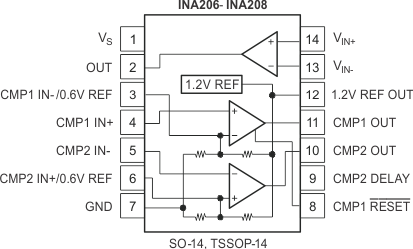
6 Pin Configuration and Functions
D or PW Packages
14-Pin SOIC OR TSSOP
Top View

Pin Functions: SOIC and TSSOP
| PIN | I/O | DESCRIPTION | |
|---|---|---|---|
| NO. | NAME | ||
| 1 | Vs | I | Power Supply |
| 2 | OUT | O | Output voltage |
| 3 | CMP1 IN-/0.6V Ref | I | Comparator 1 negative input, can be used to override the internal 0.6-V reference |
| 4 | CMP1 IN+ | I | Comparator 1 positive input |
| 5 | CMP2 IN- | I | Comparator 2 negative input |
| 6 | CMP2 IN+/0.6V Ref | I | Comparator 2 positive input, can be used to override the internal 0.6-V reference |
| 7 | GND | I | Ground |
| 8 | CMP1 RESET | I | Comparator 1 ouput reset, active low |
| 9 | CMP2 DELAY | I | Connect an optional capacitor to adjust comparator 2 delay |
| 10 | CMP2 OUT | O | Comparator 2 output |
| 11 | CMP1 OUT | O | Comparator 1 output |
| 12 | 1.2V REF OUT | O | 1.2-V reference output |
| 13 | VIN- | I | Connect to shunt low side |
| 14 | VIN+ | I | Connect to shunt high side |
DGS Package
10-Pin VSSOP
Top View

Pin Functions: VSSOP
| PIN | I/O | DESCRIPTION | |
|---|---|---|---|
| NO. | NAME | ||
| 1 | Vs | I | Power Supply |
| 2 | OUT | O | Output voltage |
| 3 | CMP1 IN+ | I | Comparator 1 positive input |
| 4 | CMP2 IN- | I | Comparator 2 negative input |
| 5 | GND | I | Ground |
| 6 | CMP1 RESET | I | Comparator 1 ouput reset, active low |
| 7 | CMP2 OUT | O | Comparator 2 output |
| 8 | CMP1 OUT | O | Comparator 1 output |
| 9 | VIN- | I | Connect to shunt low side |
| 10 | VIN+ | I | Connect to shunt high side |