SBOS247C June 2002 – November 2015 INA217
PRODUCTION DATA.
- 1 Features
- 2 Applications
- 3 Description
- 4 Revision History
- 5 Pin Configuration and Functions
- 6 Specifications
- 7 Detailed Description
- 8 Application and Implementation
- 9 Power Supply Recommendations
- 10Layout
- 11Device and Documentation Support
- 12Mechanical, Packaging, and Orderable Information
パッケージ・オプション
メカニカル・データ(パッケージ|ピン)
- DW|16
サーマルパッド・メカニカル・データ
- DW|16
発注情報
1 Features
2 Applications
- Professional Microphone Preamps
- Moving-coil Transducer Amplifiers
- Differential Receivers
- Bridge Transducer Amplifiers
3 Description
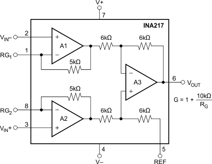
The INA217 device is a low-noise, low-distortion, monolithic instrumentation amplifier. Current-feedback circuitry allows the INA217 device to achieve wide bandwidth and excellent dynamic response over a wide range of gain. The INA217 device is ideal for low-level audio signals such as balanced low-impedance microphones. Many industrial, instrumentation, and medical applications also benefit from its low noise and wide bandwidth.
Unique distortion cancellation circuitry reduces distortion to extremely low levels, even in high gain. The INA217 device provides near-theoretical noise performance for 200-Ω source impedance. The INA217 device features differential input, low noise, and low distortion that provides superior performance in professional microphone amplifier applications.
The INA217device features wide supply voltage, excellent output voltage swing, and high output current drive, making it an optimal candidate for use in high-level audio stages.
The INA217 device is available in the same DIP-8 and SOL-16 wide body packages and pinouts as the SSM2017. For a smaller package, see the INA163 device in SO-14 narrow. The INA217 device is specified over the temperature range of –40°C to 85°C.
Device Information(1)
| PART NUMBER | PACKAGE | BODY SIZE (NOM) |
|---|---|---|
| INA217 | SOIC (16) | 10.30 mm × 7.50 mm |
| PDIP (8) | 9.81 mm × 6.35 mm |
- For all available packages, see the orderable addendum at the end of the data sheet.
Simplified Schematic
