JAJSFB6D April 2018 – July 2022 INA180-Q1 , INA2180-Q1 , INA4180-Q1
PRODMIX
- 1 特長
- 2 アプリケーション
- 3 概要
- 4 Revision History
- 5 Device Comparison
- 6 Pin Configuration and Functions
- 7 Specifications
- 8 Detailed Description
- 9 Application and Implementation
- 10Device and Documentation Support
8.4.3 Shutdown Mode
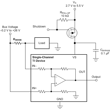
Although the INAx180-Q1 do not have a shutdown pin, the low power consumption of the device allows the output of a logic gate or transistor switch to power the INAx180-Q1. This gate or switch turns on and off the INAx180-Q1 power-supply quiescent current.
However, in current shunt monitoring applications, there is also a concern for how much current is drained from the shunt circuit in shutdown conditions. Evaluating this current drain involves considering the simplified schematic of the INAx180-Q1 in shutdown mode, as shown in Figure 8-6.
 Figure 8-6 Basic Circuit to Shut Down the INxA180-Q1
There is typically more than 500 kΩ of impedance (from the combination of 500-kΩ feedback and
input gain set resistors) from each input of the INAx180-Q1 to the OUT pin and to the GND pin. The amount of current flowing through these pins depends on the voltage at the connection.
Regarding the 500-kΩ path to the output pin, the output stage of a disabled INAx180-Q1 does constitute a good path to ground. Consequently, this current is directly proportional to a shunt common-mode voltage present across a 500-kΩ resistor.
As a final note, as long as the shunt common-mode voltage is greater than VS when the device is powered up, there is an additional and well-matched 55-µA typical current that flows in each of the inputs. If less than VS, the common-mode input currents are negligible, and the only current effects are the result of the 500-kΩ resistors.