JAJSN53A February 2012 – December 2021 INA230
PRODUCTION DATA
- 1 特長
- 2 アプリケーション
- 3 概要
- 4 Revision History
- 5 Related Products
- 6 Pin Configuration and Functions
- 7 Specifications
-
8 Detailed Description
- 8.1 Overview
- 8.2 Functional Block Diagram
- 8.3 Feature Description
- 8.4 Device Functional Modes
- 8.5 Programming
- 8.6
Register Maps
- 8.6.1 Configuration Register (00h, Read/Write)
- 8.6.2 AVG Bit Settings [11:9]
- 8.6.3 VBUS CT Bit Settings [8:6]
- 8.6.4 VSH CT Bit Settings [5:3]
- 8.6.5 Mode Settings [2:0]
- 8.6.6
Data Output Register
- 8.6.6.1 Shunt Voltage Register (01h, Read-Only)
- 8.6.6.2 Bus Voltage Register (02h, Read-Only) (1)
- 8.6.6.3 Power Register (03h, Read-Only)
- 8.6.6.4 Current Register (04h, Read-Only)
- 8.6.6.5 Calibration Register (05h, Read/Write)
- 8.6.6.6 Mask/Enable Register (06h, Read/Write)
- 8.6.6.7 Alert Limit Register (07h, Read/Write)
- 9 Application and Implementation
- 10Power Supply Recommendations
- 11Layout
- 12Device and Documentation Support
- 13Mechanical, Packaging, and Orderable Information
パッケージ・オプション
メカニカル・データ(パッケージ|ピン)
サーマルパッド・メカニカル・データ
- RGT|16
発注情報
7.7 Typical Characteristics
At TA = +25°C, VS = +3.3 V,VIN+ = 12 V, VSENSE = (VIN+ – VIN–) = 0 mV, and VBUS = 12 V, unless otherwise noted.
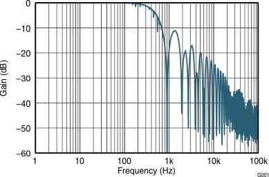
 Figure 7-1 Frequency Response
 Figure 7-3 Shunt Input Offset Voltage vs. Temperature
Figure 7-5 Shunt
Input Gain Error Production Distribution
 Figure 7-7 Shunt
Input Gain Error vs. Common-Mode Voltage
Figure 7-7 Shunt
Input Gain Error vs. Common-Mode VoltageFigure 7-9 Bus
Input Offset Voltage vs. Temperature
 Figure 7-11 Bus Input Gain Error vs. Temperature
 Figure 7-13 Input Bias Current (IB+ + IB-)
vs. Temperature
 Figure 7-15 Active IQ vs. Temperature
 Figure 7-17 Active IQ vs. I2C Clock Frequency
Figure 7-2 Shunt
Input Offset Voltage Production Distribution
 Figure 7-4 Shunt Input Common-Mode Rejection Ratio vs. Temperature
 Figure 7-6 Shunt
Input Gain Error vs. Temperature
Figure 7-6 Shunt
Input Gain Error vs. TemperatureFigure 7-8 Bus
Input Offset Voltage Production Distribution
Figure 7-10 Bus
Input Gain Error Production Distribution
 Figure 7-12 Input
Bias Current (IB+ + IB-) vs. Common-Mode
Voltage
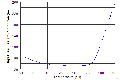
 Figure 7-14 Input Bias Current vs. Temperature, Shutdown
 Figure 7-16 Shutdown IQ vs. Temperature
 Figure 7-18 Shutdown IQ vs. I2C Clock Frequency