SBOS401C July 2007 – April 2016 INA270A-Q1 , INA271A-Q1
PRODUCTION DATA.
- 1 Features
- 2 Applications
- 3 Description
- 4 Revision History
- 5 Device Comparison Table
- 6 Pin Configuration and Functions
- 7 Specifications
- 8 Detailed Description
- 9 Application and Implementation
- 10Power Supply Recommendations
- 11Layout
- 12Device and Documentation Support
- 13Mechanical, Packaging, and Orderable Information
1 Features
- Qualified for Automotive Applications
- AEC-Q100 Qualified With the Following Results:
- Device Temperature Grade 1: –40°C to +125°C Ambient Operating Temperature Range
- Device HBM ESD Classification Level 2
- Device CDM ESD Classification Level C6
- Pinout Optimized for External Filtering
- Wide Common-Mode Range: –16 V to +80 V
- Accuracy:
- CMRR: 120 dB
- ±2.5-mV Offset (Maximum)
- ±1% Gain Error (Maximum)
- 20-μV/°C Offset Drift (Maximum)
- 55-ppm/°C Gain Drift (Maximum)
- Bandwidth: Up to 130 kHz
- Two Gain Options Available:
- 14 V/V (INA270A-Q1)
- 20 V/V (INA271A-Q1)
- Quiescent Current: 900 μA (Maximum)
- Power Supply: 2.7 V to 18 V
- Packages: SOIC-8
2 Applications
- Electric Power Steering (EPS) Systems
- Body Control Modules
- Brake Systems
- Electronic Stability Control (ESC) Systems
3 Description
The INA270A-Q1 and INA271A-Q1 (INA27xA-Q1) family of current-shunt monitors with voltage output can sense voltage drops across current shunts at common-mode voltages from –16 V to +80 V, independent of the supply voltage. The INA27xA-Q1 pinouts readily enable filtering.
The INA27xA-Q1 devices are available with two output voltage scales: 14 V/V and 20 V/V. The 130-kHz bandwidth simplifies use in current-control loops.
The INA27xA-Q1 operates from a single 2.7-V to 18-V supply, drawing a maximum of 900 μA of supply current. They are specified over the extended operating temperature range of –40°C to +125°C and are offered in an SOIC-8 package.
Device Information(1)
| PART NUMBER | PACKAGE | BODY SIZE (NOM) |
|---|---|---|
| INA270A-Q1 | SOIC (8) | 4.90 mm × 3.91 mm |
| INA271A-Q1 |
- For all available packages, see the orderable addendum at the end of the data sheet.
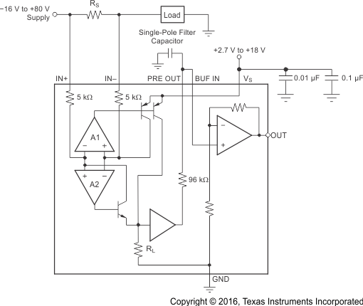
Simplified Schematic
