JAJSNR9B April   2016  – April 2022 INA301-Q1

PRODUCTION DATA  

  1. 特長
  2. アプリケーション
  3. 概要
  4. Revision History
  5. Pin Configuration and Functions
  6. Specifications
    1. 6.1 Absolute Maximum Ratings
    2. 6.2 ESD Ratings
    3. 6.3 Recommended Operating Conditions
    4. 6.4 Thermal Information
    5. 6.5 Electrical Characteristics
    6. 6.6 Typical Characteristics
  7. Detailed Description
    1. 7.1 Overview
    2. 7.2 Functional Block Diagram
    3. 7.3 Feature Description
      1. 7.3.1 Alert Output ( ALERT Pin)
      2. 7.3.2 Current-Limit Threshold
        1. 7.3.2.1 Resistor-Controlled Current Limit
          1. 7.3.2.1.1 Resistor-Controlled, Current-Limit Example
        2. 7.3.2.2 Voltage-Source-Controlled Current Limit
      3. 7.3.3 Hysteresis
    4. 7.4 Device Functional Modes
      1. 7.4.1 Alert Mode
        1. 7.4.1.1 Transparent Output Mode
        2. 7.4.1.2 Latch Output Mode
  8. Applications and Implementation
    1. 8.1 Application Information
      1. 8.1.1 Selecting a Current-Sensing Resistor
        1. 8.1.1.1 Selecting a Current-Sensing Resistor Example
      2. 8.1.2 Input Filtering
      3. 8.1.3 INA301-Q1 Operation With Common-Mode Voltage Transients Greater Than 36 V
    2. 8.2 Typical Application
      1. 8.2.1 Design Requirements
      2. 8.2.2 Detailed Design Procedure
      3. 8.2.3 Application Curve
  9. Power Supply Recommendations
  10. 10Layout
    1. 10.1 Layout Guidelines
    2. 10.2 Layout Example
  11. 11Device and Documentation Support
    1. 11.1 Documentation Support
      1. 11.1.1 Related Documentation
    2. 11.2 Receiving Notification of Documentation Updates
    3. 11.3 サポート・リソース
    4. 11.4 Trademarks
    5. 11.5 Electrostatic Discharge Caution
    6. 11.6 Glossary
  12. 12Mechanical, Packaging, and Orderable Information

パッケージ・オプション

メカニカル・データ(パッケージ|ピン)
サーマルパッド・メカニカル・データ
発注情報

INA301-Q1 Operation With Common-Mode Voltage Transients Greater Than 36 V

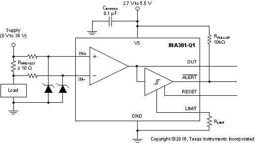
With a small amount of additional circuitry, the INA301-Q1 can be used in circuits subject to transients greater than 36 V. Use only Zener diodes or Zener-type transient absorbers (sometimes referred to as transzorbs). Any other type of transient absorber has an unacceptable time delay. Start by adding a pair of resistors as a working impedance for the Zener diode, as shown in Figure 8-3. Keep these resistors as small as possible; preferably, 10 Ω or less. Larger values can be used, but with an additional induced error resulting from less signal reaching the device input pins. Because this circuit limits only short-term transients, many applications are satisfied with a 10-Ω resistor along with conventional Zener diodes of the lowest power rating available. This combination uses the least amount of board space. These diodes can be found in packages as small as SOT-523 or SOD-523.
GUID-31DBACC8-9C04-4BCA-BA1F-55BC117C48A2-low.gifFigure 8-3 Transient Protection