JAJSCZ9C September 2016 – March 2019 INA302 , INA303
PRODUCTION DATA.
- 1 特長
- 2 アプリケーション
- 3 概要
- 4 改訂履歴
- 5 概要(続き)
- 6 Pin Configuration and Functions
- 7 Specifications
- 8 Detailed Description
- 9 Application and Implementation
- 10Power Supply Recommendations
- 11Layout
- 12デバイスおよびドキュメントのサポート
- 13メカニカル、パッケージ、および注文情報
8.3.3 Alert Outputs
Both ALERTx pins are active-low, open-drain outputs that pull low when the sensed current is detected to be out of range. Both open-drain ALERTx pins require an external pullup resistor to an external supply. The external supply for the pullup voltage can exceed the supply voltage, VS, but is restricted from operating at greater than 5.5 V. The pullup resistance is selected based on the capacitive load and required rise time; however, a 10-kΩ resistor value is typically sufficient for most applications. The response time of the ALERT1 output to an out-of-range event is less than 1 μs, and the response time of the ALERT2 output is proportional to the value of the external CDELAY capacitor. The equation to calculate the delay time for the ALERT2 output is given in Equation 2:

where
- CDELAY is the external delay capacitor.
- VTH is the delay threshold voltage.
- ID is the DELAY pin current for comparator 2.
For example, if a delay time of 10 µs is desired, the calculated value for CDELAY is 492 pF. The closest standard capacitor value to the calculated value is 500 pF. If a delay time greater than 2.5 µs on the ALERT2 output is not needed, the CDELAY capacitor can be omitted. To achieve minimum delay on the ALERT2 output, connect a 100-kΩ resistor from the DELAY pin to the VS pin. Both comparators in the INA30x have hysteresis to avoid oscillations in the ALERTx outputs. The effect hysteresis has on the comparator behavior is described in the Hysteresis section.
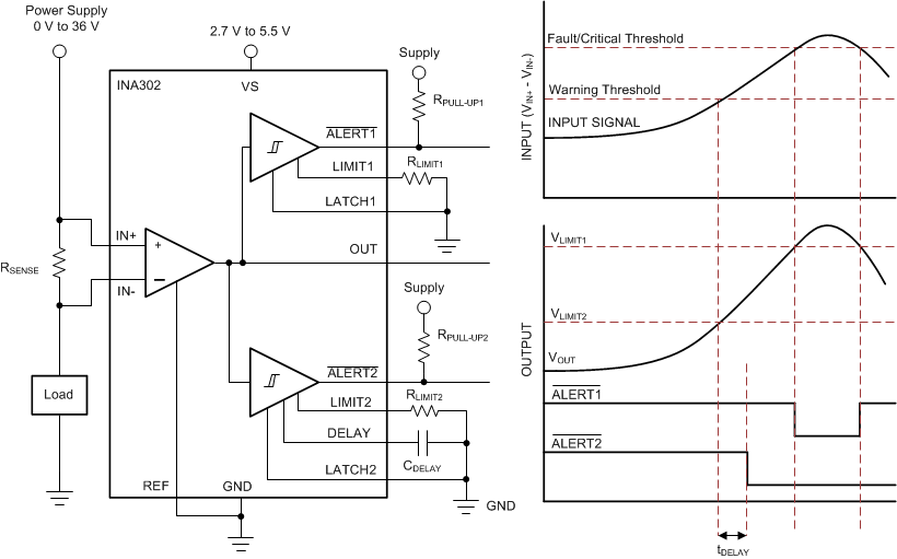
Figure 42 shows the alert output response of the internal comparators for the INA302. When the output voltage of the current-sense amplifier is less than the voltage developed on either limit pin, both ALERTx outputs are in the default high state. When the current sense amplifier output is greater than the threshold voltage set by the LIMIT2 pin, the ALERT2 output pulls low after a delay time set by the external delay capacitor. The lower overcurrent threshold is commonly referred to as the overcurrent warning threshold. If the current continues to rise until the current-sense amplifier output voltage exceeds the threshold voltage set at the LIMIT1 pin, then the ALERT1 output becomes active and immediately pulls low. The low voltage on ALERT1 indicates that the measured signal at the amplifier input has exceeded the programmed threshold level, indicating an overcurrent condition has occurred. The upper threshold is commonly referred to as the fault or system critical threshold. Systems often initiate protection procedures (such as a system shutdown) when the current exceeds this threshold.
 Figure 42. Out-of-Range Alert Responses for the INA302
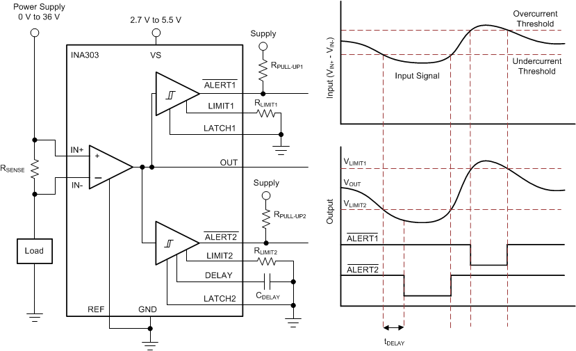
 Figure 43 shows the alert output response of the internal comparators for the INA303. Both ALERTx outputs are in the default high state when the output voltage of the current-sense amplifier is less than the voltage developed at the LIMIT1 pin and is greater than the voltage developed at the LIMIT2 pin. The ALERT1 output becomes active and pulls low when the current-sense amplifier output voltage exceeds the threshold voltage set at the LIMIT1 pin. The low voltage on ALERT1 indicates that the measured signal at the amplifier input has exceeded the programmed threshold level, indicating an overcurrent or out-of-range condition has occurred. When the current-sense amplifier output is less than the threshold voltage set by the LIMIT2 pin, the ALERT2 output pulls low after the delay time set by the external delay capacitor expires. The delay time for the ALERT2 output is proportional to the value of the external CDELAY capacitor, and is calculated by Equation 2.
 Figure 43. Out-of-Range Alert Responses for the INA303
 Figure 44 shows the alert output response of the INA303 when the two ALERTx pins are connected together. When configured in this manner, the INA303 can provide a single signal to indicate when the sensed current is operating either outside the normal operating bands or within a normal operational window. Both ALERT1 and ALERT2 outputs behave the same in regard to the alert mode. The difference with ALERT2 is that the transition of the output state is delayed by the time set by the external delay capacitor. If the overcurrent or undercurrent event is not present when the delay time expires, ALERT2 does not respond.
 Figure 44. Current Window Comparator Implementation With the INA303