JAJSCL8B May 2012 – March 2016 INA3221
PRODUCTION DATA.
- 1 特長
- 2 アプリケーション
- 3 概要
- 4 改訂履歴
- 5 Device Comparison Table
- 6 Pin Configuration and Functions
- 7 Specifications
-
8 Detailed Description
- 8.1 Overview
- 8.2 Functional Block Diagram
- 8.3 Feature Description
- 8.4 Device Functional Modes
- 8.5 Programming
- 8.6
Register Maps
- 8.6.1 Summary of Register Set
- 8.6.2
Register Descriptions
- 8.6.2.1 Configuration Register (address = 00h) [reset = 7127h]
- 8.6.2.2 Channel-1 Shunt-Voltage Register (address = 01h), [reset = 00h]
- 8.6.2.3 Channel-1 Bus-Voltage Register (address = 02h) [reset = 00h]
- 8.6.2.4 Channel-2 Shunt-Voltage Register (address = 03h) [reset = 00h]
- 8.6.2.5 Channel-2 Bus-Voltage Register (address = 04h) [reset = 00h]
- 8.6.2.6 Channel-3 Shunt-Voltage Register (address = 05h) [reset = 00h]
- 8.6.2.7 Channel-3 Bus-Voltage Register (address = 06h) [reset = 00h]
- 8.6.2.8 Channel-1 Critical-Alert Limit Register (address = 07h) [reset = 7FF8h]
- 8.6.2.9 Warning-Alert Channel-1 Limit Register (address = 08h) [reset = 7FF8h]
- 8.6.2.10 Channel-2 Critical-Alert Limit Register (address = 09h) [reset = 7FF8h]
- 8.6.2.11 Channel-2 Warning-Alert Limit Register (address = 0Ah) [reset = 7FF8h]
- 8.6.2.12 Channel-3 Critical-Alert Limit Register (address = 0Bh) [reset = 7FF8h]
- 8.6.2.13 Channel-3 Warning-Alert Limit Register (address = 0Ch) [reset = 7FF8h]
- 8.6.2.14 Shunt-Voltage Sum Register (address = 0Dh) [reset = 00h]
- 8.6.2.15 Shunt-Voltage Sum-Limit Register (address = 0Eh) [reset = 7FFEh]
- 8.6.2.16 Mask/Enable Register (address = 0Fh) [reset = 0002h]
- 8.6.2.17 Power-Valid Upper-Limit Register (address = 10h) [reset = 2710h]
- 8.6.2.18 Power-Valid Lower-Limit Register (address = 11h) [reset = 2328h]
- 8.6.2.19 Manufacturer ID Register (address = FEh) [reset = 5449h]
- 8.6.2.20 Die ID Register (address = FFh) [reset = 3220]
- 9 Application and Implementation
- 10Power Supply Recommendations
- 11Layout
- 12デバイスおよびドキュメントのサポート
- 13メカニカル、パッケージ、および注文情報
パッケージ・オプション
メカニカル・データ(パッケージ|ピン)
- RGV|16
サーマルパッド・メカニカル・データ
- RGV|16
発注情報
7 Specifications
7.1 Absolute Maximum Ratings
over operating free-air temperature range (unless otherwise noted)(1)| MIN | MAX | UNIT | |||
|---|---|---|---|---|---|
| Voltage | Supply, VS | 6 | V | ||
| Analog inputs | IN+, IN– | Differential (VIN+) – (VIN–)(2) | –26 | 26 | V |
| Common-mode (VIN+) + (VIN–) / 2 | –0.3 | 26 | |||
| VPU | 26 | ||||
| Digital outputs | Critical, warning, power valid | 6 | V | ||
| Timing control | 26 | ||||
| Serial bus | Data line, SDA | (GND – 0.3) | 6 | V | |
| Clock line, SCL | (GND – 0.3) | (VS + 0.3) | |||
| Current | Input, into any pin | 5 | mA | ||
| Open-drain, digital output | 10 | ||||
| Temperature | Operating, TA | –40 | 125 | °C | |
| Junction, TJ | 150 | ||||
| Storage, Tstg | –65 | 150 | |||
(1) Stresses beyond those listed under Absolute Maximum Ratings may cause permanent damage to the device. These are stress ratings only, which do not imply functional operation of the device at these or any other conditions beyond those indicated under Recommended Operating Conditions. Exposure to absolute-maximum-rated conditions for extended periods may affect device reliability.
(2) VIN+ and VIN– can have a differential voltage of –26 V to +26 V; however, the voltage at these pins must not exceed the range of
–0.3 V to +26 V.
–0.3 V to +26 V.
7.2 ESD Ratings
| VALUE | UNIT | |||
|---|---|---|---|---|
| V(ESD) | Electrostatic discharge | Human-body model (HBM), per ANSI/ESDA/JEDEC JS-001(1) | ±2500 | V |
| Charged-device model (CDM), per JEDEC specification JESD22-C101(2) | ±1000 | |||
| Machine model | ±200 | |||
(1) JEDEC document JEP155 states that 500-V HBM allows safe manufacturing with a standard ESD control process.
(2) JEDEC document JEP157 states that 250-V CDM allows safe manufacturing with a standard ESD control process.
7.3 Recommended Operating Conditions
over operating free-air temperature range (unless otherwise noted)| MIN | NOM | MAX | UNIT | ||
|---|---|---|---|---|---|
| Operating supply voltage | 2.7 | 5.5 | V | ||
| Operating temperature, TA | –40 | 125 | °C | ||
7.4 Thermal Information
| THERMAL METRIC(1) | INA3221 | UNIT | |
|---|---|---|---|
| RGV (VQFN) | |||
| 16 PINS | |||
| RθJA | Junction-to-ambient thermal resistance | 36.5 | °C/W |
| RθJC(top) | Junction-to-case (top) thermal resistance | 42.7 | °C/W |
| RθJB | Junction-to-board thermal resistance | 14.7 | °C/W |
| ψJT | Junction-to-top characterization parameter | 0.5 | °C/W |
| ψJB | Junction-to-board characterization parameter | 14.8 | °C/W |
| RθJC(bot) | Junction-to-case (bottom) thermal resistance | 3.3 | °C/W |
(1) 従来および新しい熱測定値の詳細については、『Semiconductor and IC Package Thermal Metrics』アプリケーション・レポート(SPRA953)を参照してください。
7.5 Electrical Characteristics
at TA = 25°C, VS = 3.3 V, VIN+ = 12 V, VSHUNT = (VIN+) – (VIN–) = 0 mV, and VBUS = VIN– = 12 V (unless otherwise noted)| PARAMETER | TEST CONDITIONS | MIN | TYP | MAX | UNIT | ||
|---|---|---|---|---|---|---|---|
| INPUT | |||||||
| VSHUNT | Shunt voltage input | –163.84 | 163.8 | mV | |||
| VBUS | Bus voltage input | 0 | 26 | V | |||
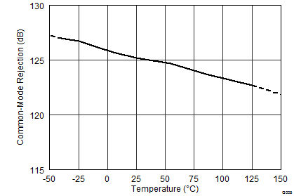
| CMR | Common-mode rejection | VIN+ = 0 V to +26 V | 110 | 120 | dB | ||
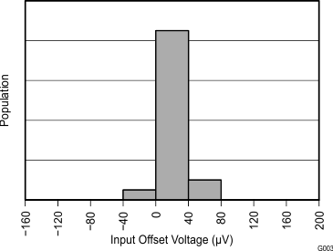
| VOS | Shunt offset voltage, RTI(1) | ±40 | ±80 | μV | |||
| TA = –40°C to +125°C | 0.1 | 0.5 | μV/°C | ||||
| PSRR | vs power supply, VS = 2.7 V to 5.5 V | 15 | μV/V | ||||
| VOS | Bus offset voltage, RTI(1) | ±8 | ±16 | mV | |||
| TA = –40°C to +125°C | 80 | μV/°C | |||||
| PSRR | vs power supply | 0.5 | mV/V | ||||
| IIN+ | Input bias current at IN+ | 10 | μA | ||||
| IIN– | Input bias current at IN– | 10 || 670 | μA || kΩ | ||||
| Input leakage(2) | (IN+ pin) + (IN– pin), power-down mode | 0.1 | 0.5 | μA | |||
| DC ACCURACY | |||||||
| ADC native resolution | 13 | Bits | |||||
| 1-LSB step size | Shunt voltage | 40 | μV | ||||
| Bus voltage | 8 | mV | |||||
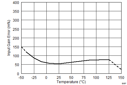
| Shunt voltage gain error | 0.1% | 0.25% | |||||
| TA = –40°C to +125°C | 10 | 50 | ppm/°C | ||||
| Bus voltage gain error | 0.1% | 0.25% | |||||
| TA = –40°C to +125°C | 10 | 50 | ppm/°C | ||||
| DNL | Differential nonlinearity | ±0.1 | LSB | ||||
| tCONVERT | ADC conversion time | CT bit = 000 | 140 | 154 | µs | ||
| CT bit = 001 | 204 | 224 | |||||
| CT bit = 010 | 332 | 365 | |||||
| CT bit = 011 | 588 | 646 | |||||
| CT bit = 100 | 1.1 | 1.21 | ms | ||||
| CT bit = 101 | 2.116 | 2.328 | |||||
| CT bit = 110 | 4.156 | 4.572 | |||||
| CT bit = 111 | 8.244 | 9.068 | |||||
| SMBus | |||||||
| SMBus timeout(3) | 28 | 35 | ms | ||||
| DIGITAL INPUT/OUTPUT | |||||||
| CI | Input capacitance | 3 | pF | ||||
| Leakage input current | 0 V ≤ VIN ≤ VS | 0.1 | 1 | μA | |||
| VIH | High-level input voltage | 0.7 (VS) | 6 | V | |||
| VIL | Low-level input voltage | –0.5 | 0.3 (VS) | V | |||
| VOL | Low-level output voltage | SDA, critical, warning, PV | VS > +2.7 V, IOL = 3 mA | 0 | 0.4 | V | |
| TC | VS > +2.7 V, IOL = 1.2 mA | 0 | 0.4 | ||||
| Vhys | Hysteresis voltage | 500 | mV | ||||
| POWER SUPPLY | |||||||
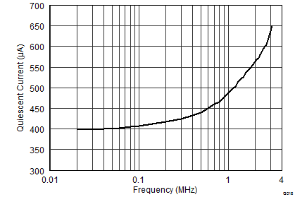
| Quiescent current | 350 | 450 | μA | ||||
| Power-down mode | 0.5 | 2 | |||||
| Power-on reset threshold | 2 | V | |||||
(1) RTI = Referred-to-input.
(2) Input leakage is positive (current flows into the pin) for the conditions shown at the top of this table. Negative leakage currents can occur under different input conditions.
(3) SMBus timeouts in the INA3221 reset the interface whenever SCL is low for more than 28 ms.
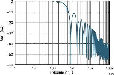
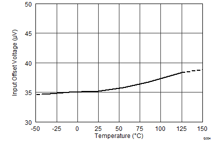
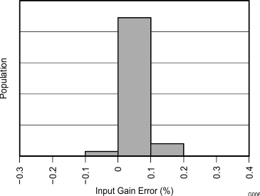
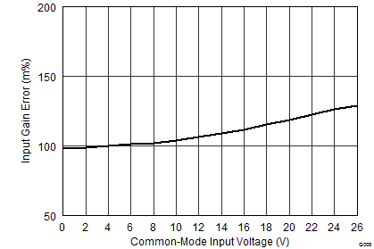
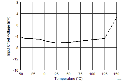
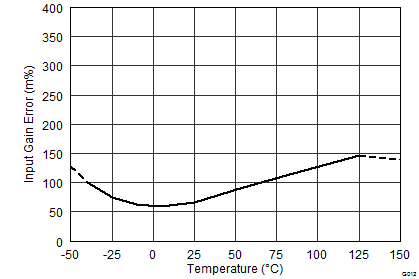
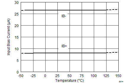
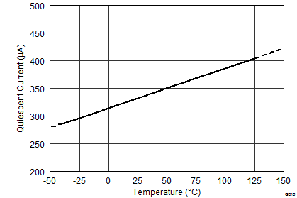
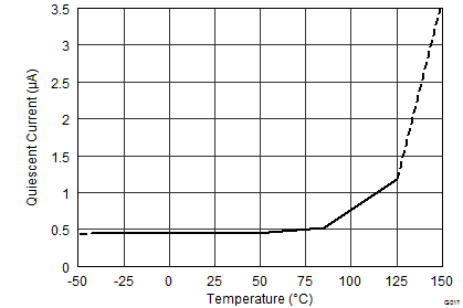
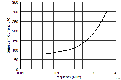
7.6 Typical Characteristics
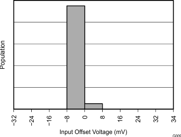
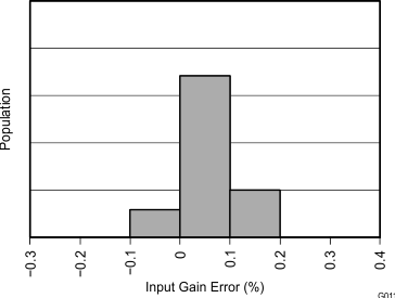
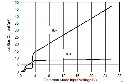
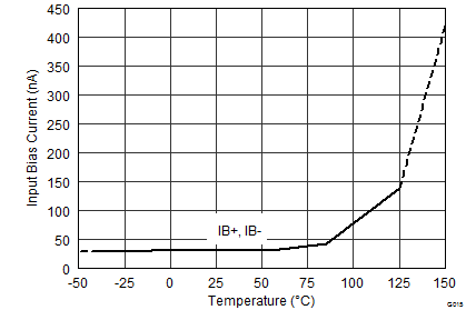
at TA = 25°C, VS = 3.3 V, VIN+ = 12 V, VSHUNT = (VIN+) – (VIN–) = 0 mV, and VBUS = VIN– = 12 V (unless otherwise noted)