JAJSPA2D December 2022 – November 2024 INA351
PRODUCTION DATA
- 1
- 1 特長
- 2 アプリケーション
- 3 概要
- 4 Device Comparison Table
- 5 Pin Configuration and Functions
- 6 Specifications
- 7 Detailed Description
- 8 Application and Implementation
- 9 Device and Documentation Support
- 10Revision History
- 11Mechanical, Packaging, and Orderable Information
パッケージ・オプション
メカニカル・データ(パッケージ|ピン)
サーマルパッド・メカニカル・データ
- DSG|8
発注情報
8.1.2 Input Bias Current Return Path
The input impedance of the INA351 is extremely high, but a path must be provided for the input bias current of both inputs. This input bias current is typically a few pico amps but at high temperature this can be a few nano amps. High input impedance means that the input bias current changes little with varying input voltage.
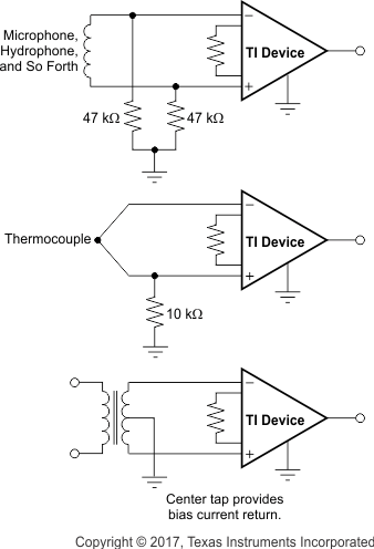
For proper operation, input circuitry must provide a path for this input bias current. Figure 8-3 shows various provisions for an input bias current path. Without a bias current path, the inputs float to a potential that exceeds the common-mode range of the INA351, and the input amplifiers saturate. If the differential source resistance is low, the bias current return path connects to one input (as shown in the thermocouple example in Figure 8-3). With a higher source impedance, use two equal resistors to provide a balanced input, with the possible advantages of a lower input offset voltage as a result of bias current, and better high-frequency common-mode rejection.
 Figure 8-3 Providing an
Input Common-Mode Current Path