at TA = 25°C,
VS = (V+) – (V–) = 5.5 V, VIN = (VIN+) –
(VIN–) = 0 V, RL = 10 kΩ, CL = 10 pF,
VREF = VS / 2, VCM = [(VIN+) +
(VIN–)] / 2 = VS / 2, VOUT = VS / 2
and G = 10 (unless otherwise noted)
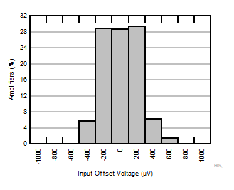
| G = 10, 20, 30, 50 |
N = 36 |
μ = 23 μV |
σ = 0.180 mV |
Figure 6-1 Typical Distribution of Input Referred Offset Voltage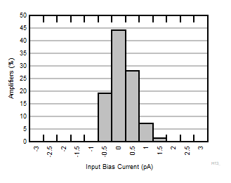
| TA = 25°C |
N = 72 |
μ = 0.33 pA |
σ = 0.43 pA |
Figure 6-3 Typical Distribution of Input Bias Current 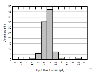
| TA = 85°C |
N = 72 |
μ = 3.3 pA |
σ = 0.53 pA |
Figure 6-5 Typical Distribution of Input Bias Current 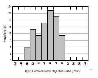
| G = 10 |
N = 36 |
μ = -0.30 μV/V |
σ = 7.10 μV/V |
Figure 6-7 Typical Distribution of CMRR 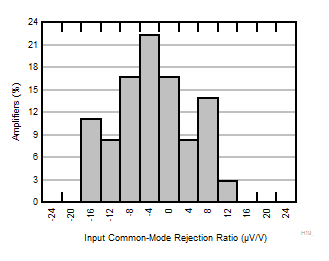
| G = 30 |
N = 36 |
μ = –1.23 μV/V |
σ = 7.52 μV/V |
Figure 6-9 Typical Distribution of CMRR 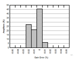
| G = 10 |
N = 36 |
μ = 0.002 % |
σ = 0.02 % |
Figure 6-11 Typical Distribution of Gain
Error 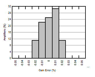
| G = 30 |
N = 36 |
μ = 0.0067 % |
σ = 0.011 % |
Figure 6-13 Typical Distribution of Gain Error 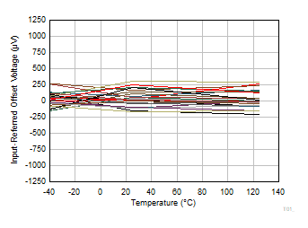 Figure 6-15 Input
Referred Offset Voltage vs Temperature
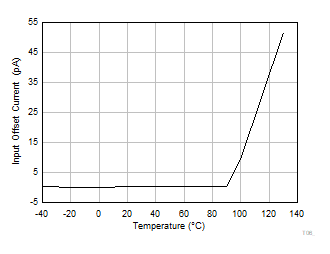 Figure 6-17 Input
Offset Current vs Temperature
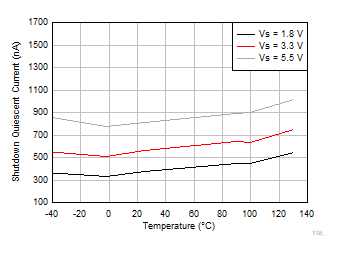 Figure 6-19 Shutdown Quiescent Current vs Temperature
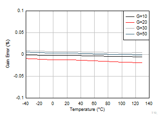 Figure 6-21 Gain
Error vs Temperature
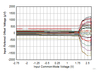
| V+ =
2.75 V and V– = –2.75 V |
Figure 6-23 Input
Referred Offset Voltage vs Input Common-Mode Voltage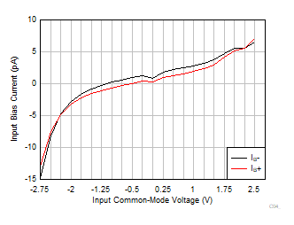
| V+ =
2.75 V and V– = –2.75 V |
Figure 6-25 Input
Bias Current vs Input Common-Mode Voltage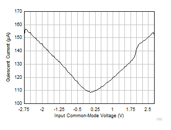
| V+ =
2.75 V and V– = –2.75 V |
Figure 6-27 Quiescent Current vs Input Common-Mode Voltage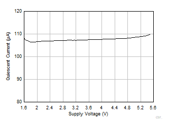 Figure 6-29 Quiescent Current vs Supply Voltage
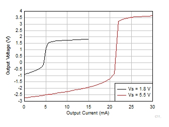 Figure 6-31 Output Voltage vs Output Current (Sinking)
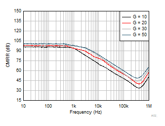 Figure 6-33 CMRR
(Referred to Input) vs Frequency
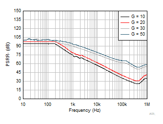 Figure 6-35 PSRR–
(Referred to Input) Vs Frequency
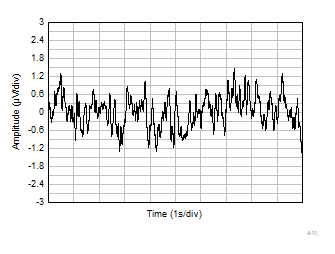 Figure 6-37 0.1
Hz to 10 Hz Voltage Noise in Time Domain
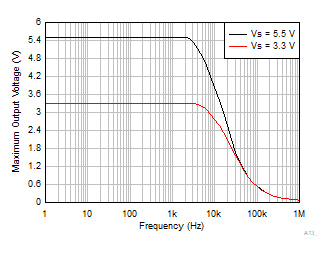 Figure 6-39 Maximum Output Voltage vs Frequency
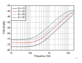
| VS = 5.5 V |
BW = 80 kHz |
VCM = 2.75 V |
| RL = 100 kΩ |
VOUT = 1
VRMS |
|
Figure 6-41 THD + N Frequency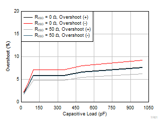
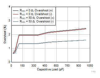
| VS = 5.5 V |
G = 10 |
VOUT = 100
mVPP |
Figure 6-43 Small-Signal Overshoot vs
Capacitive Load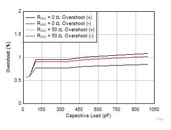
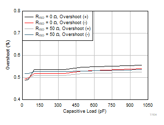
| VS = 5.5 V |
G = 30 |
VOUT = 100
mVPP |
Figure 6-45 Small-Signal Overshoot vs Capacitive Load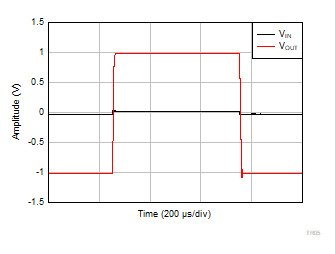
| V+ = 2.75 V |
V– = –2.75 V |
G = 10 |
VOUT = 2
VPP |
Figure 6-47 Large
Signal Step Response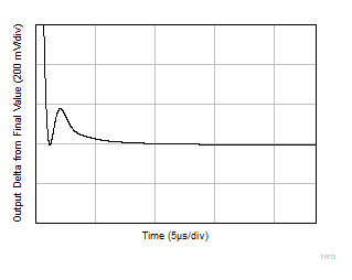
| V+ = 2.75 V |
V– = –2.75 V |
G = 10 |
VOUT = 2
VPP |
Figure 6-49 Large Signal Settling Time
(Rising Edge)
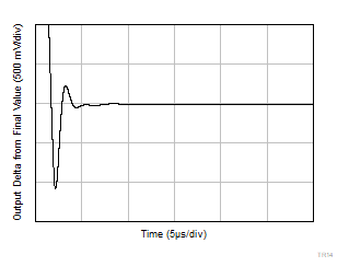
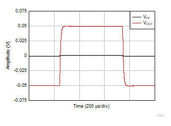
| V+ = 2.75 V |
V– = –2.75 V |
G = 10 |
VOUT = 0.1
VPP |
Figure 6-51 Small-Signal Step
Response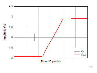
| V+ = 2.75 V |
V– = –2.75 V |
G = 10 |
VIN = 1
VPP |
Figure 6-53 Over-Load Recovery (Rising Edge)
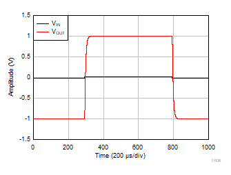
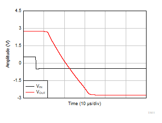
| V+ = 2.75 V |
V– = –2.75 V |
G = 10 |
VIN = 0.6
VPP |
Figure 6-55 No
Phase Reversal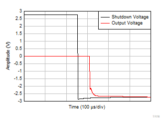
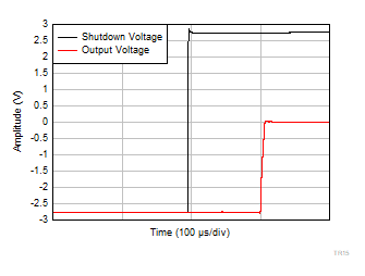
| V+ = +2.75 V |
V– = –2.75 V |
G = 10 |
Figure 6-57 Disable Response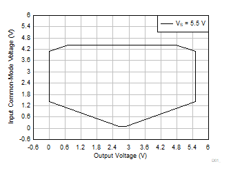
| VS = 5.5 V |
G = 10, 20, 30, 50 |
VREF = VS / 2 |
Figure 6-59 Input
Common-Mode Voltage vs Output Voltage (High CMRR Region)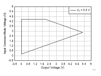
| VS = 5.5 V |
G = 10, 20, 30, 50 |
VREF = 0 V |
Figure 6-61 Input
Common-Mode Voltage vs Output Voltage (High CMRR Region)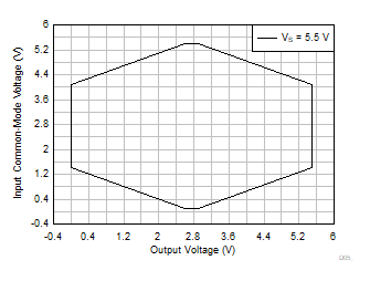
| VS = 5.5 V |
G = 10, 20, 30, 50 |
VREF = VS / 2 |
Figure 6-63 Input
Common-Mode Voltage vs Output Voltage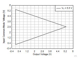
| VS = 5.5 V |
G = 10, 20, 30, 50 |
VREF = 0 V |
Figure 6-65 Input Common-Mode Voltage vs
Output Voltage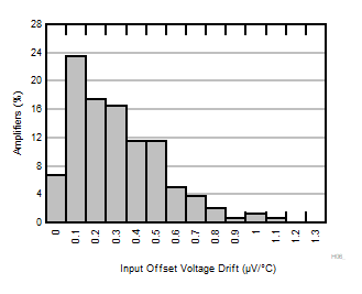
|
G = 10, 20, 30, 50 |
N = 36 |
μ = 0.23 μV/°C |
σ = 0.36 μV/°C |
Figure 6-2 Typical Distribution of Input Referred Offset Drift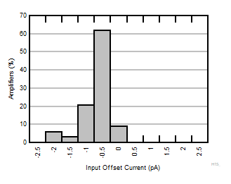
| TA = 25°C |
N = 36 |
μ = –0.40 pA |
σ = 0.47 pA |
Figure 6-4 Typical Distribution of Input Offset Current 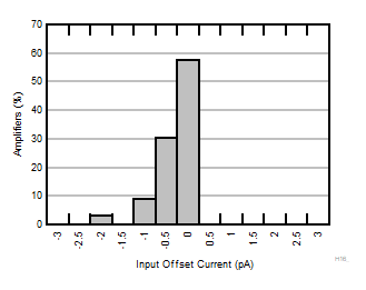
| TA = 85°C |
N = 36 |
μ = 0.05 pA |
σ = 0.30 pA |
Figure 6-6 Typical Distribution of Input Offset Current 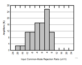
| G = 20 |
N = 36 |
μ = -0.27 μV/V |
σ = 7.20 μV/V |
Figure 6-8 Typical Distribution of CMRR 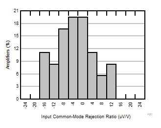
| G = 50 |
N = 36 |
μ = –1.16 μV/V |
σ = 7.62 μV/V |
Figure 6-10 Typical Distribution of CMRR 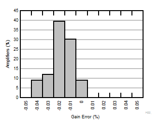
| G = 20 |
N = 36 |
μ = -0.02 % |
σ = 0.02 % |
Figure 6-12 Typical Distribution of Gain Error 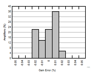
| G = 50 |
N = 36 |
μ = 0.0035 % |
σ = 0.012 % |
Figure 6-14 Typical Distribution of Gain Error 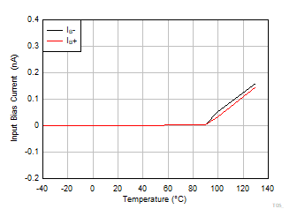 Figure 6-16 Input
Bias Current vs Temperature
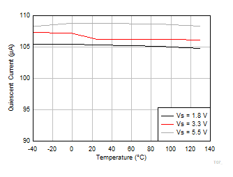 Figure 6-18 Quiescent Current vs Temperature
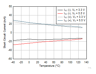 Figure 6-20 Short
Circuit Current vs Temperature
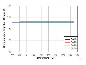 Figure 6-22 CMRR
vs Temperature
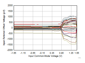
| V+ =
1.65 V and V– = –1.65 V |
Figure 6-24 Input
Referred Offset Voltage vs Input Common-Mode Voltage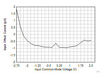
| V+ =
2.75 V and V– = –2.75 V |
Figure 6-26 Input
Offset Current vs Input Common-Mode Voltage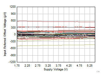 Figure 6-28 Input
Referred Offset Voltage vs Supply Voltage
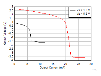 Figure 6-30 Output Voltage vs Output Current (Sourcing)
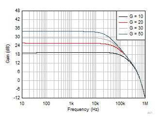 Figure 6-32 Closed-Loop Gain vs Frequency
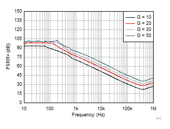 Figure 6-34 PSRR+
(Referred to Input) vs Frequency
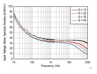 Figure 6-36 Input
Referred Voltage Noise Spectral Density
 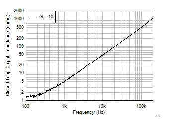 Figure 6-38 Closed-Loop Output Impedance vs Frequency
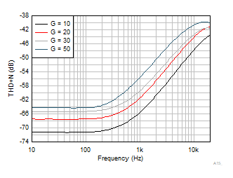
| VS = 5.5 V |
BW = 80 kHz |
VCM = 2.75 V |
| RL = 10 kΩ |
VOUT = 0.5
VRMS |
|
Figure 6-40 THD +
N Frequency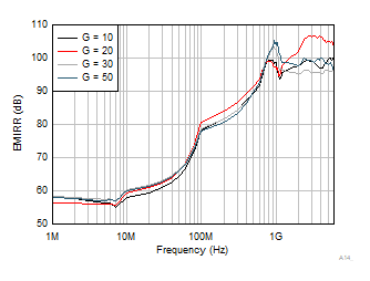 Figure 6-42 Electromagnetic Interference
Rejection Ratio Referred to Noninverting Input (EMIRR+) vs Frequency
| VS = 5.5 V |
G = 20 |
VOUT = 100
mVPP |
Figure 6-44 Small-Signal Overshoot vs
Capacitive Load
| VS = 5.5 V |
G = 50 |
VOUT = 100
mVPP |
Figure 6-46 Small-Signal Overshoot vs Capacitive Load
| V+ = 2.75 V |
V– = –2.75 V |
G = 10 |
VOUT = 2
VPP |
Figure 6-48 Large Signal Settling Time
(Falling Edge)
| V+ = 2.75 V |
V– = –2.75 V |
G = 50 |
VOUT = 2
VPP |
Figure 6-50 Large Signal Step
Response
| V+ = 2.75 V |
V– = –2.75 V |
G = 50 |
VOUT = 0.1
VPP |
Figure 6-52 Small-Signal Step Response
| V+ = 2.75 V |
V– = –2.75 V |
G = 10 |
VIN = 1
VPP |
Figure 6-54 Over-Load Recovery (Falling Edge)
| V+ = +2.75 V |
V– = –2.75 V |
G = 10 |
Figure 6-56 Enable Response
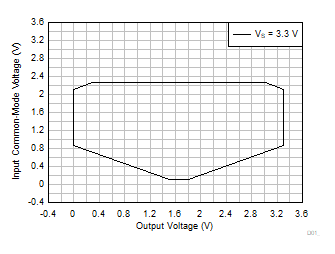
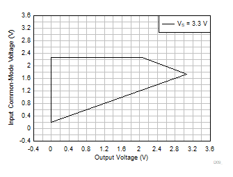
| VS = 3.3 V |
G = 10, 20, 30, 50 |
VREF = VS / 2 |
Figure 6-58 Input
Common-Mode Voltage vs Output Voltage (High CMRR Region)
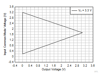
| VS = 3.3 V |
G = 10, 20, 30, 50 |
VREF = 0 V |
Figure 6-60 Input
Common-Mode Voltage vs Output Voltage (High CMRR Region)
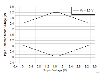
| VS = 3.3 V |
G = 10, 20, 30, 50 |
VREF = VS / 2 |
Figure 6-62 Input
Common-Mode Voltage vs Output Voltage
| VS = 3.3 V |
G = 10, 20, 30, 50 |
VREF = 0 V |
Figure 6-64 Input Common-Mode Voltage vs
Output Voltage


 Figure 6-17 Input
Offset Current vs Temperature
 Figure 6-19 Shutdown Quiescent Current vs Temperature
 Figure 6-21 Gain
Error vs Temperature


 Figure 6-31 Output Voltage vs Output Current (Sinking)
 Figure 6-33 CMRR
(Referred to Input) vs Frequency
 Figure 6-35 PSRR–
(Referred to Input) Vs Frequency
 Figure 6-37 0.1
Hz to 10 Hz Voltage Noise in Time Domain
 Figure 6-39 Maximum Output Voltage vs Frequency


 Figure 6-16 Input
Bias Current vs Temperature
 Figure 6-18 Quiescent Current vs Temperature
 Figure 6-20 Short
Circuit Current vs Temperature
 Figure 6-22 CMRR
vs Temperature


 Figure 6-30 Output Voltage vs Output Current (Sourcing)
 Figure 6-32 Closed-Loop Gain vs Frequency
 Figure 6-34 PSRR+
(Referred to Input) vs Frequency
 Figure 6-36 Input
Referred Voltage Noise Spectral Density
  Figure 6-38 Closed-Loop Output Impedance vs Frequency
 Figure 6-42 Electromagnetic Interference
Rejection Ratio Referred to Noninverting Input (EMIRR+) vs Frequency