JAJSEX6B December   2017  – October 2019 INA381

PRODUCTION DATA.  

  1. 特長
  2. アプリケーション
  3. 概要
    1.     Device Images
      1.      代表的なアプリケーション
  4. 改訂履歴
  5. 概要(続き)
  6. Pin Configuration and Functions
    1.     Pin Functions
  7. Specifications
    1. 7.1 Absolute Maximum Ratings
    2. 7.2 ESD Ratings
    3. 7.3 Recommended Operating Conditions
    4. 7.4 Thermal Information
    5. 7.5 Electrical Characteristics
    6. 7.6 Typical Characteristics
  8. Detailed Description
    1. 8.1 Overview
    2. 8.2 Functional Block Diagram
    3. 8.3 Feature Description
      1. 8.3.1 Wide Input Common-Mode Voltage Range
      2. 8.3.2 Precise Low-Side Current Sensing
      3. 8.3.3 High Bandwidth and Slew Rate
      4. 8.3.4 Alert Output
      5. 8.3.5 Adjustable Overcurrent Threshold
      6. 8.3.6 Comparator Hysteresis
    4. 8.4 Device Functional Modes
      1. 8.4.1 Alert Modes
        1. 8.4.1.1 Transparent Output Mode
        2. 8.4.1.2 Latch Output Mode
  9. Applications and Implementation
    1. 9.1 Application Information
      1. 9.1.1 Select a Current-Sensing Resistor
        1. 9.1.1.1 Select a Current-Sensing Resistor: Example
      2. 9.1.2 Increase Comparator Hysteresis
      3. 9.1.3 Operation With Common-Mode Transients Greater Than 26 V
      4. 9.1.4 Input Filtering
    2. 9.2 Typical Applications
      1. 9.2.1 Bidirectional Window Comparator
        1. 9.2.1.1 Design Requirements
        2. 9.2.1.2 Detailed Design Procedure
        3. 9.2.1.3 Application Curve
      2. 9.2.2 Solenoid Low-Side Current Sensing
        1. 9.2.2.1 Design Requirements
        2. 9.2.2.2 Detailed Design Procedure
        3. 9.2.2.3 Application Curve
  10. 10Power Supply Recommendations
  11. 11Layout
    1. 11.1 Layout Guidelines
    2. 11.2 Layout Example
  12. 12デバイスおよびドキュメントのサポート
    1. 12.1 ドキュメントのサポート
      1. 12.1.1 関連資料
    2. 12.2 ドキュメントの更新通知を受け取る方法
    3. 12.3 サポート・リソース
    4. 12.4 商標
    5. 12.5 静電気放電に関する注意事項
    6. 12.6 Glossary
  13. 13メカニカル、パッケージ、および注文情報

パッケージ・オプション

デバイスごとのパッケージ図は、PDF版データシートをご参照ください。

メカニカル・データ(パッケージ|ピン)
  • DGS|10
  • DSG|8
サーマルパッド・メカニカル・データ
発注情報

Adjustable Overcurrent Threshold

The VOUT voltage is the amplified voltage developed across the current-sensing resistor. The signal developed at the VOUT pin is the input voltage across the IN+ and IN– pins multiplied by the gain of the amplifier. The INA381 has four gain options, as shown in Figure 42: 20 V/V, 50 V/V, 100 V/V, and 200 V/V. If additional hysteresis is not required, directly connect the VOUT pin to the CMPIN pin.
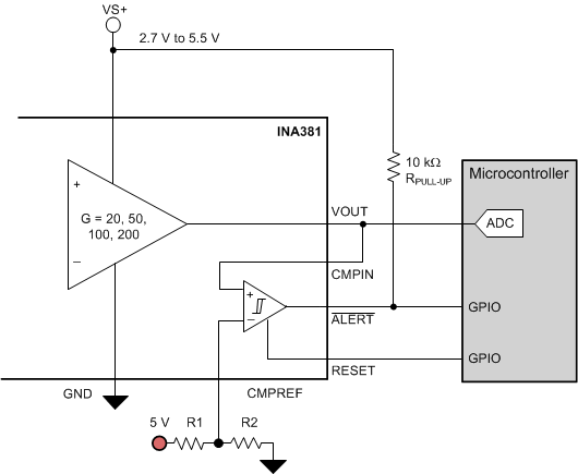
INA381 SettingCurThresho.gifFigure 42. Resistor Divider Voltage

The device determines if an overcurrent event is present by comparing the voltage on the CMPIN pin to the corresponding signal developed at the CMPREF pin. The threshold voltage for the CMPREF pin can be set with a resistive divider, or by connecting an external voltage source (such as a reference generator device). Figure 43 depicts the REF3140 used as an external reference source.
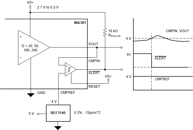
INA381 ina381-external-reference-voltage.gifFigure 43. External Reference Voltage