SBOS562G
August 2011 – June 2020
INA826
PRODUCTION DATA.
1
Features
2
Applications
3
Description
Device Images
General-Purpose Instrumentation Amplifier
4
Revision History
5
Device Comparison Table
6
Pin Configuration and Functions
Pin Functions
7
Specifications
7.1
Absolute Maximum Ratings
7.2
ESD Ratings
7.3
Recommended Operating Conditions
7.4
Thermal Information
7.5
Electrical Characteristics
7.6
Typical Characteristics
8
Detailed Description
8.1
Overview
8.2
Functional Block Diagram
8.3
Feature Description
8.3.1
Inside the INA826
8.3.2
Setting the Gain
8.3.2.1
Gain Drift
8.3.3
Offset Trimming
8.3.4
Input Common-Mode Range
8.3.5
Input Protection
8.3.6
Input Bias Current Return Path
8.3.7
Reference Terminal
8.3.8
Dynamic Performance
8.3.9
Operating Voltage
8.3.9.1
Low-Voltage Operation
8.3.10
Error Sources
8.4
Device Functional Modes
9
Application and Implementation
9.1
Application Information
9.2
Typical Application
9.2.1
Design Requirements
9.2.2
Detailed Design Procedure
9.2.3
Application Curves
9.3
System Examples
9.3.1
Circuit Breaker
9.3.2
Programmable Logic Controller (PLC) Input
9.3.3
Using TINA-TI SPICE-Based Analog Simulation Program With the INA826
10
Power Supply Recommendations
11
Layout
11.1
Layout Guidelines
11.1.1
CMRR vs Frequency
11.2
Layout Example
12
Device and Documentation Support
12.1
Documentation Support
12.1.1
Related Documentation
12.2
Receiving Notification of Documentation Updates
12.3
Support Resources
12.4
Trademarks
12.5
Electrostatic Discharge Caution
12.6
Glossary
13
Mechanical, Packaging, and Orderable Information
パッケージ・オプション
メカニカル・データ(パッケージ|ピン)
D|8
MSOI002K
DRG|8
MPDS151B
DGK|8
MPDS028E
サーマルパッド・メカニカル・データ
DRG|8
QFND084H
発注情報
sbos562g_oa
sbos562g_pm
7.6
Typical Characteristics
at T
A
= 25°C, V
S
= ±15 V, R
L
= 10 kΩ, V
REF
= 0 V, and G = 1 (unless otherwise noted)
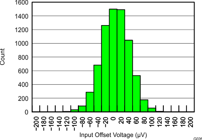
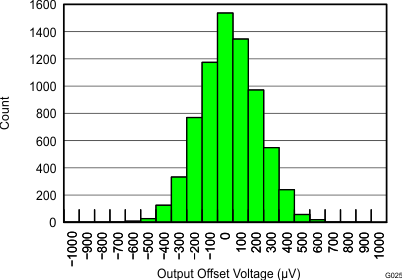
Figure 1.
Typical Distribution of Input Offset Voltage
Figure 3.
Typical Distribution of Output Offset Voltage
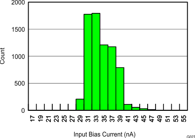
Figure 5.
Typical Distribution of Input Bias Current
G = 1
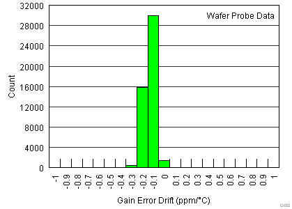
Figure 7.
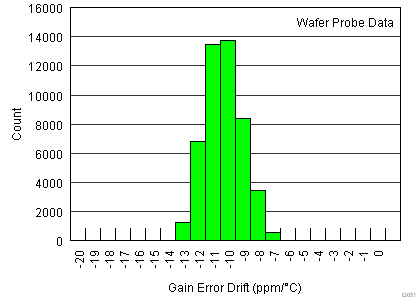
Typical Gain Error Drift Distribution
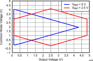
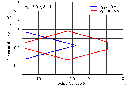
Single supply
Figure 9.
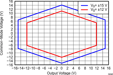
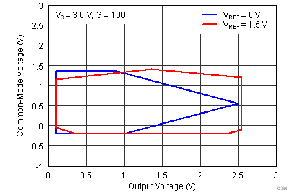
Input Common-Mode Voltage vs Output Voltage
Single supply
Figure 11.
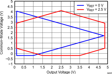
Input Common-Mode Voltage vs Output Voltage
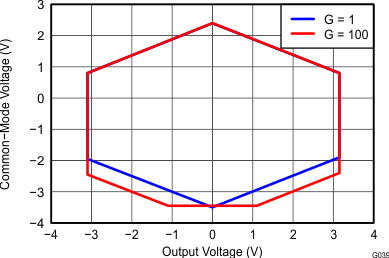
Dual supply
Figure 13.
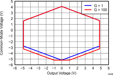
Input Common-Mode Voltage vs Output Voltage
Dual supply
Figure 15.
Input Common-Mode Voltage vs Output Voltage
G = 1
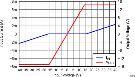
Figure 17.
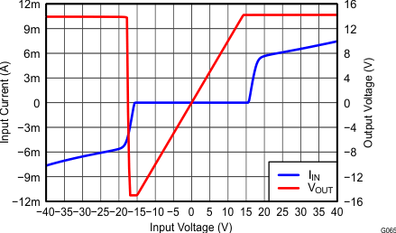
Input Overvoltage vs Input Current
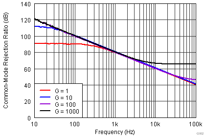
Figure 19.
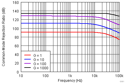
CMRR vs Frequency (RTI)
Figure 21.
Positive PSRR vs Frequency (RTI)
Figure 23.
Gain vs Frequency
Figure 25.
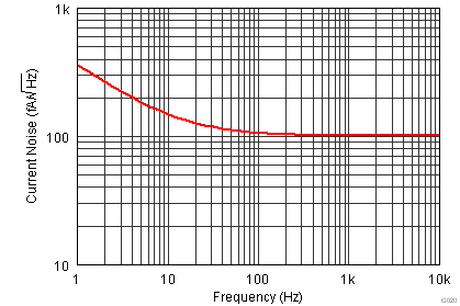
Current Noise Spectral Density vs Frequency (RTI)
G = 1000
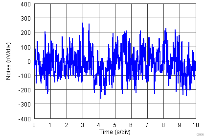
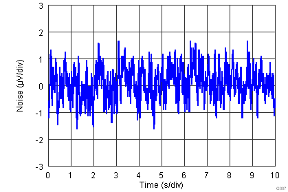
Figure 27.
0.1-Hz to 10-Hz RTI Voltage Noise
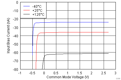
V
S
= 3.0 V
Figure 29.
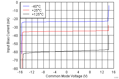
Input Bias Current vs Common-Mode Voltage
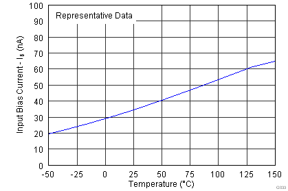
Figure 31.
Input Bias Current vs Temperature
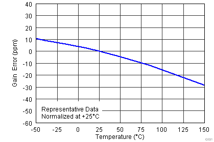
G = 1
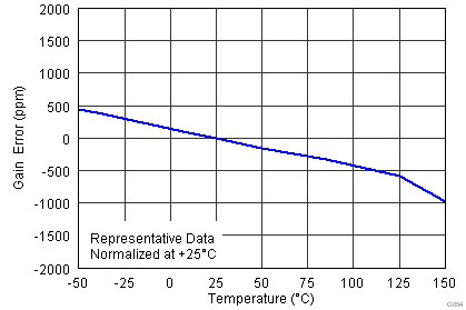
Figure 33.
Gain Error vs Temperature
G = 1
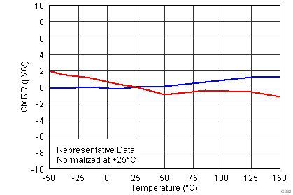
Figure 35.
CMRR vs Temperature
G = 1
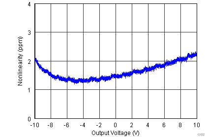
Figure 37.
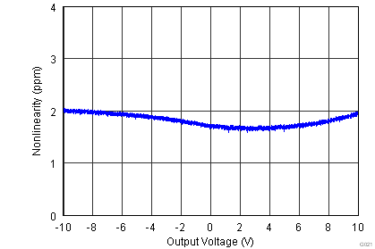
Gain Nonlinearity
G = 100
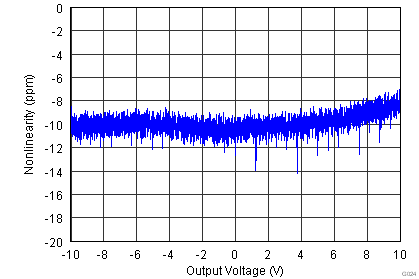
Figure 39.
Gain Nonlinearity
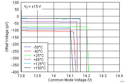
Figure 41.
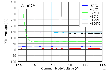
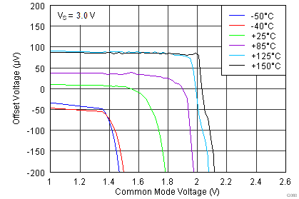
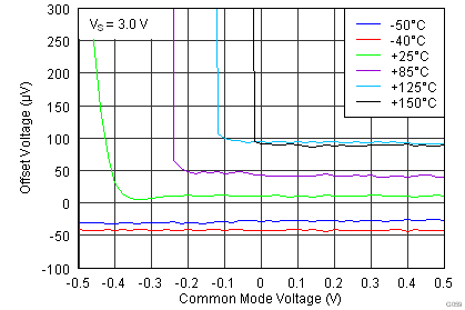
Offset Voltage vs Negative Common-Mode Voltage
Figure 43.
Offset Voltage vs Negative Common-Mode Voltage
Figure 45.
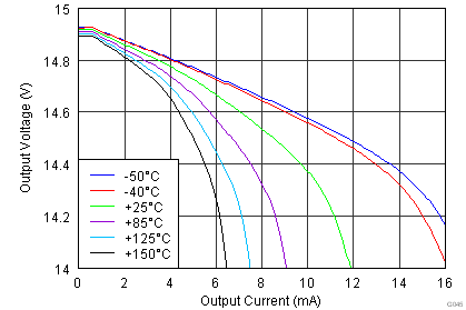
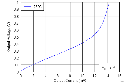
Positive Output Voltage Swing vs Output Current
Figure 47.
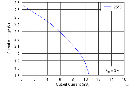
Positive Output Voltage Swing vs Output Current
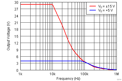
Figure 49.
Large-Signal Frequency Response
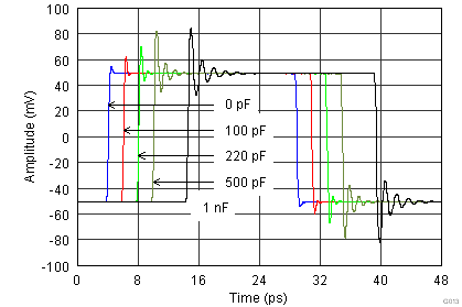
G = 1
Figure 51.
Small-Signal Response Over Capacitive Loads
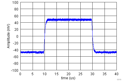
G = 10, R
L
= 10 kΩ, C
L
= 100 pF
Figure 53.
Small-Signal Response
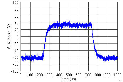
G = 1000, R
L
= 10 kΩ, C
L
= 100 pF
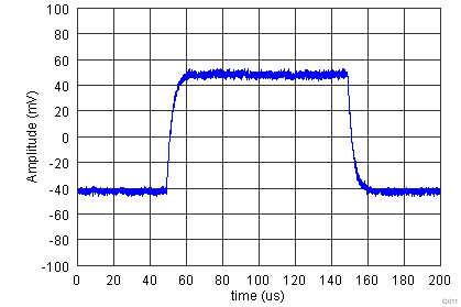
Figure 55.
Small-Signal Response
Figure 57.
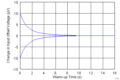
Change in Input Offset Voltage vs Warm-Up Time
Figure 2.
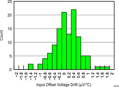
Typical Distribution of Input Offset Voltage Drift
Figure 4.
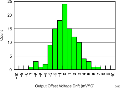
Typical Distribution of Output Offset Voltage Drift
Figure 6.
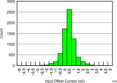
Typical Distribution of Input Offset Current
G > 1
Figure 8.
Typical Gain Error Drift Distribution
Single supply
Figure 10.
Input Common-Mode Voltage vs Output Voltage
Single supply
Figure 12.
Input Common-Mode Voltage vs Output Voltage
Dual supply
Figure 14.
Input Common-Mode Voltage vs Output Voltage
Dual supply
Figure 16.
Input Common-Mode Voltage vs Output Voltage
G = 1
Figure 18.
Input Overvoltage vs Input Current
With 10-kΩ Resistance
Figure 20.
CMRR vs Frequency
(RTI, 1-kΩ Source Imbalance)
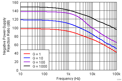
Figure 22.
Negative PSRR vs Frequency (RTI)
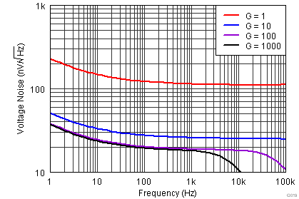
Figure 24.
Voltage Noise Spectral Density
vs Frequency (RTI)
G = 1
Figure 26.
0.1-Hz to 10-Hz RTI Voltage Noise
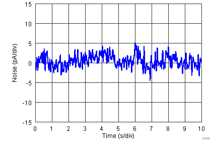
Figure 28.
0.1-Hz to 10-Hz RTI Current Noise
Figure 30.
Input Bias Current vs Common-Mode Voltage
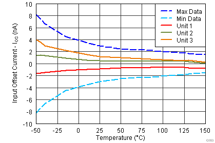
Figure 32.
Input Offset Current vs Temperature
G > 1
Figure 34.
Gain Error vs Temperature
Figure 36.
Supply Current vs Temperature
G = 10
Figure 38.
Gain Nonlinearity
G = 1000
Figure 40.
Gain Nonlinearity
Figure 42.
Offset Voltage vs Positive Common-Mode Voltage
Figure 44.
Offset Voltage vs Positive Common-Mode Voltage
Figure 46.
Negative Output Voltage Swing vs Output Current
Figure 48.
Negative Output Voltage Swing vs Output Current
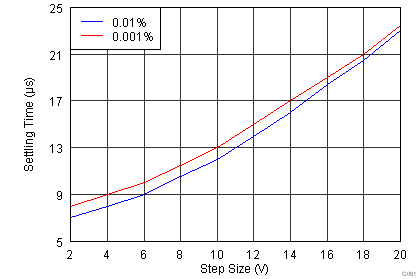
Figure 50.
Settling Time vs Step Size
G = 1, R
L
= 1 kΩ, C
L
= 100 pF
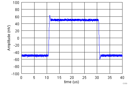
Figure 52.
Small-Signal Response
G = 100, R
L
= 10 kΩ, C
L
= 100 pF
Figure 54.
Small-Signal Response
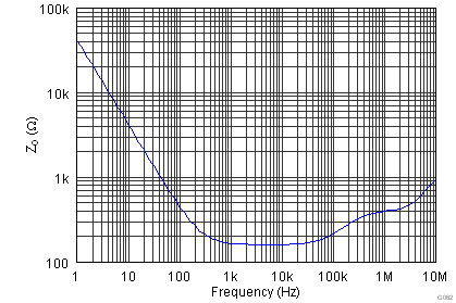
Figure 56.
Open-Loop Output Impedance