JAJSD55A May 2017 – June 2017 INA826S
PRODUCTION DATA.
- 1 特長
- 2 アプリケーション
- 3 概要
- 4 改訂履歴
- 5 Pin Configuration and Functions
- 6 Specifications
- 7 Detailed Description
- 8 Application and Implementation
- 9 Power Supply Recommendations
- 10Layout
- 11デバイスおよびドキュメントのサポート
- 12メカニカル、パッケージ、および注文情報
パッケージ・オプション
メカニカル・データ(パッケージ|ピン)
- DRC|10
サーマルパッド・メカニカル・データ
- DRC|10
発注情報
7 Detailed Description
7.1 Overview
A simplified schematic of the INA826S is shown in as well as the basic connections required for proper functionality. The INA826S consists of a 4-resistor difference amplifier, composed of amplifier A3 and 50-kΩ resistors, as well as buffer amplifiers A1 and A2. The gain of the circuit is set by a single external resistor placed across pins 2 and 3. Further information on the internal topology and setting the gain can be found in the Feature Description section. High-precision thin-film resistors integrated on-chip allow for excellent rejection of common-mode interference signals and high gain accuracy. The INA826S also integrates radio frequency interference (RFI) filters on the signal inputs to provide improved performance in the presence of high-frequency interference.
7.2 Functional Block Diagram

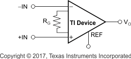 Figure 64. INA826S Basic Connections
7.3 Feature Description
7.3.1 Inside the INA826S
See the Functional Block Diagram section for a simplified representation of the INA826S. A more detailed diagram (shown in Figure 65) provides additional details of the INA826S operation.
Each input is protected by two field-effect transistors (FETs) that provide a low series resistance under normal signal conditions, and preserve excellent noise performance. When excessive voltage is applied, these transistors limit input current to approximately 8 mA.
The differential input voltage is buffered by Q1 and Q2 and is impressed across RG, causing a signal current to flow through RG, R1, and R2. The output difference amplifier, A3, removes the common-mode component of the input signal and refers the output signal to the REF pin.
The equations shown in Figure 65 describe the output voltages of A1 and A2. The VBE and voltage drop across R1 and R2 produce output voltages on A1 and A2 that are approximately 0.8 V higher than the input voltages.
 Figure 65. INA826S Simplified Circuit Diagram
7.3.2 Setting the Gain
Gain of the INA826S is set by a single external resistor, RG, connected between pins 2 and 3. Use Equation 1 to select the value of RG:

Table 1 lists several commonly-used gains and resistor values. The 49.4-kΩ term in Equation 1 comes from the sum of the two internal 24.7-kΩ feedback resistors. These on-chip resistors are laser-trimmed to accurate absolute values. The accuracy and temperature coefficients of these resistors are included in the gain accuracy and drift specifications of the INA826S.
Table 1. Commonly-Used Gains and Resistor Values
| DESIRED GAIN (V/V) | RG (Ω) | NEAREST 1% RG (Ω) |
|---|---|---|
| 1 | — | — |
| 2 | 49.4 k | 49.9 k |
| 5 | 12.35 k | 12.4 k |
| 10 | 5.489 k | 5.49 k |
| 20 | 2.600 k | 2.61 k |
| 50 | 1.008 k | 1 k |
| 100 | 499 | 499 |
| 200 | 248 | 249 |
| 500 | 99 | 100 |
| 1000 | 49.5 | 49.9 |
7.3.2.1 Gain Drift
The stability and temperature drift of the external gain setting resistor, RG, also affects gain. The contribution of RG to gain accuracy and drift can be directly inferred from the gain of Equation 1.
The best gain drift of 1 ppm/℃ can be achieved when the INA826S uses G = 1 without RG connected. In this case, the gain drift is limited only by the slight mismatch of the temperature coefficient of the integrated 50-kΩ resistors in the differential amplifier (A3). At G greater than 1, the gain drift increases as a result of the individual drift of the 24.7-kΩ resistors in the feedback of A1 and A2, relative to the drift of the external gain resistor RG. Process improvements of the temperature coefficient of the feedback resistors now make possible specifying a maximum gain drift of the feedback resistors of 35 ppm/℃, thus significantly improving the overall temperature stability of applications using gains greater than 1.
Low resistor values required for high gain can make wiring resistance important. Sockets add to the wiring resistance and contribute additional gain error (such as a possible unstable gain error) at gains of approximately 100 or greater. To ensure stability, avoid parasitic capacitance of more than a few picofarads at RG connections. Careful matching of any parasitics on both RG pins maintains optimal CMRR over frequency; see typical characteristic curves Figure 22 and Figure 23.
7.3.3 Offset Trimming
Most applications require no external offset adjustment; however, if necessary, adjustments can be made by applying a voltage to the REF pin. Figure 66 shows an optional circuit for trimming the output offset voltage. The voltage applied to the REF pin is summed at the output. The op amp buffer provides low impedance at the REF pin to preserve good common-mode rejection.
 Figure 66. Optional Trimming of Output Offset Voltage
7.3.4 Input Common-Mode Range
The linear input voltage range of the INA826S input circuitry extends from the negative supply voltage to 1 V below the positive supply, and maintains 84-dB (minimum) common-mode rejection throughout this range. The common-mode range for most common operating conditions is described in Figure 12 through Figure 18 and Figure 44 through Figure 46. The INA826S can operate over a wide range of power supplies and VREF configurations, making a comprehensive guide to common-mode range limits impractical to be provided for all possible conditions.
The most commonly overlooked overload condition occurs when a circuit exceeds the output swing of A1 and A2, which are internal circuit nodes that cannot be measured. Calculating the expected voltages at the output of A1 and A2 (see Figure 65) provides a check for the most common overload conditions. The designs of A1 and A2 are identical and the outputs can swing to within approximately 100 mV of the power-supply rails. For example, when the A2 output is saturated, A1 may continue to be in linear operation, responding to changes in the noninverting input voltage. This difference can give the appearance of linear operation but the output voltage is invalid.
A single-supply instrumentation amplifier has special design considerations. To achieve a common-mode range that extends to single-supply ground, the INA826S employs a current-feedback topology with PNP input transistors; see Figure 65. The matched PNP transistors Q1 and Q2 shift the input voltages of both inputs up by a diode drop, and through the feedback network, shift the output of A1 and A2 by approximately 0.8 V. With both inputs and VREF at single-supply ground (negative power supply), the output of A1 and A2 is well within the linear range, allowing differential measurements to be made at the GND level. As a result of this input level-shifting, the voltages at pin 2 and pin 3 are not equal to the respective input pin voltages (pin 1 and pin 4). For most applications, this inequality is not important because only the gain-setting resistor connects to these pins.
7.3.5 Input Protection
The inputs of the INA826S are individually protected for voltages up to ±40 V. For example, a condition of –40 V on one input and 40 V on the other input does not cause damage. However, if the input voltage exceeds (V–) – 2 V and the signal source current drive capability exceeds 3.5 mA, the output voltage switches to the opposite polarity; see Figure 20. This polarity reversal can easily be avoided by adding resistance of 10 kΩ in series with both inputs.
Internal circuitry on each input provides low series impedance under normal signal conditions. If the input is overloaded, the protection circuitry limits the input current to a safe value of approximately 8 mA. Figure 20 and Figure 21 illustrate this input current limit behavior. The inputs are protected even if the power supplies are disconnected or turned off.
7.3.6 Input Bias Current Return Path
The input impedance of the INA826S is extremely high—approximately 20 GΩ. However, a path must be provided for the input bias current of both inputs. This input bias current is typically 35 nA. High input impedance means that this input bias current changes very little with varying input voltage.
Input circuitry must provide a path for this input bias current for proper operation. Figure 67 shows various provisions for an input bias current path. Without a bias current path, the inputs float to a potential that exceeds the common-mode range of the INA826S, and the input amplifiers saturate. If the differential source resistance is low, as shown in the thermocouple example in Figure 67, the bias current return path can be connected to one input. With higher source impedance, using two equal resistors provides a balanced input with possible advantages of lower input offset voltage as a result of bias current and better high-frequency common-mode rejection.
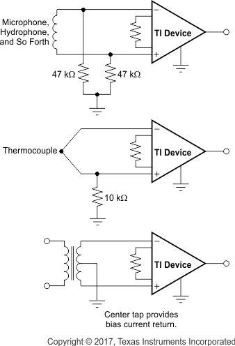 Figure 67. Providing an Input Common-Mode Current Path
7.3.7 Reference Pin (REF)
The output voltage of the INA826S is developed with respect to the voltage on the reference terminal. Often, in dual-supply operation, the reference pin (pin 6) is connected to the low-impedance system ground. In single-supply operation, offsetting the output signal to a precise mid-supply level can be useful (for example, 2.5 V in a 5-V supply environment). To accomplish this offset, a voltage source can be tied to the REF pin to level-shift the output so that the INA826S can drive a single-supply ADC, for example.
For the best performance, keep the source impedance to the REF pin below 5 Ω. As shown in , the reference resistor is at one end of a 50-kΩ resistor. Additional impedance at the REF pin adds to this 50-kΩ resistor. The imbalance in the resistor ratios results in degraded common-mode rejection ratio (CMRR).
Figure 68 shows two different methods of driving the reference pin with low impedance. The OPA330 is a low-power, chopper-stabilized amplifier, and therefore offers excellent stability over temperature. The OPA330 is available in the space-saving SC70 and even smaller chip-scale package. The REF3225 is a precision reference in the small SOT23-6 package.
 Figure 68. Options for Low-Impedance Level Shifting
7.3.8 Shutdown (EN and ENREF) Pins
The INA826S provides two pins to shut the device down: EN (enable) and ENREF (enable reference). Figure 69 shows a basic schematic of the shutdown logic circuitry of the INA826S. A PNP transistor forms the basis of the internal shutdown circuitry. The ENREF pin is connected to the emitter of the PNP transistor and is meant to be connected to a voltage reference point for the enable logic. The EN pin is connected the base of the PNP transistor. Applying a voltage to the EN pin that is 0.8 V or more below the enable reference voltage (at the ENREF pin) causes a small current to flow in the internal PNP transistor that powers the INA826S internal bias circuitry and powers-up the instrumentation amplifier. The shutdown circuitry functions properly with ENREF connected to a voltage between (V–) + 1.5 V up to V+. The voltage on the EN pin can be as low as the negative supply voltage (VS–) but cannot go above the voltage applied to the ENREF pin.
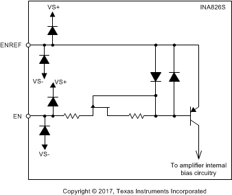 Figure 69. Shutdown Pin Simplified Schematic
To better understand the functionality of these pins, consider the low-voltage, single-supply application shown in Figure 70 with V+ = 3.3 V. ENREF is connected to the 3.3-V power supply of the microcontroller (labeled µC) and the EN pin is toggled by a general-purpose input/output (GPIO) pin of the microcontroller. When the GPIO pin is asserted low, such that the voltage at the GPIO pin output is at or near 0 V, the INA826S is enabled. Conversely, if the GPIO pin is asserted high, with an output voltage at or near 3.3 V, the INA826S is disabled.
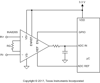 Figure 70. Example Configuration in a Single-Supply System
(Pulling EN low enables the INA826S.)
Figure 71 shows an alternate configuration of the enable logic pins. By grounding the enable pin, and toggling the ENREF pin with the GPIO of the microcontroller, the enable logic is reversed. Now asserting high at the GPIO output enables the INA826S, and pulling the GPIO pin low disables the INA826S.
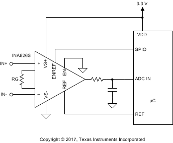 Figure 71. Alternate Configuration for the Enable Logic Pins
(Pulling ENREF high enables the INA826S.)
The majority of INA826S applications benefit greatly from the reduction of quiescent current from the typical 200 µA to values at or below 6 µA. Achieving the lowest possible system-level current in a system requires attention to other system voltages applied to the INA826S. When shutdown, voltages applied to the reference or input pins of the INA826S can find paths for currents to flow up into the several microamps region. In many systems these voltages are shut down when the INA826S is shutdown, simplifying the problem. Otherwise, additional switching may be added to reduce currents to a minimum.
7.4 Device Functional Modes
The INA826S features a shutdown mode that reduces the typical power-supply current consumption from 200 µA to less than 6 µA. Disabling the INA826S turns off the bias circuitry that powers the internal amplifiers of the INA826S. Figure 72 and Figure 73 show the output behavior of the INA826S when the shutdown state is toggled. For these plots, the ENREF pin was connected to a 5-V potential and the EN pin was pulled low to enable the INA826S. Figure 72 shows how quickly the INA826S output responds when transitioning from a shutdown state to an enabled state. When the EN pin is pulled low, the INA826S output begins to track the input signal approximately 60 µs later. When transitioning from enabled to shutdown, as shown in Figure 73, the output of the INA826S stops tracking the input waveform in approximately 10 µs.
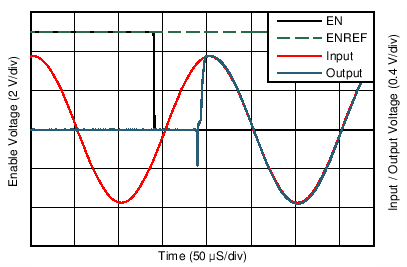 Figure 72. Enable Output Response
 Figure 73. Disable Output Response