SBOS631B June   2012  – November 2017 INA827

PRODUCTION DATA.  

  1. Features
  2. Applications
  3. Description
  4. Revision History
  5. Pin Configuration and Functions
  6. Specifications
    1. 6.1 Absolute Maximum Ratings
    2. 6.2 ESD Ratings
    3. 6.3 Recommended Operating Conditions
    4. 6.4 Thermal Information
    5. 6.5 Electrical Characteristics
  7. Typical Characteristics
  8. Detailed Description
    1. 8.1 Overview
    2. 8.2 Functional Block Diagram
    3. 8.3 Feature Description
      1. 8.3.1  Setting the Gain
        1. 8.3.1.1 Gain Drift
      2. 8.3.2  Offset Trimming
      3. 8.3.3  Input Common-Mode Range
      4. 8.3.4  Inside the INA827
      5. 8.3.5  Input Protection
      6. 8.3.6  Input Bias Current Return Path
      7. 8.3.7  Reference Pin
      8. 8.3.8  Dynamic Performance
      9. 8.3.9  Operating Voltage
        1. 8.3.9.1 Low-Voltage Operation
      10. 8.3.10 Error Sources
    4. 8.4 Device Functional Modes
  9. Application and Implementation
    1. 9.1 Application Information
    2. 9.2 Typical Application
      1. 9.2.1 Design Requirements
      2. 9.2.2 Detailed Design Procedure
      3. 9.2.3 Application Curves
  10. 10Power Supply Recommendations
  11. 11Layout
    1. 11.1 Layout Guidelines
      1. 11.1.1 CMRR vs Frequency
    2. 11.2 Layout Example
  12. 12Device and Documentation Support
    1. 12.1 Documentation Support
      1. 12.1.1 Related Documentation
    2. 12.2 Receiving Notification of Documentation Updates
    3. 12.3 Community Resources
    4. 12.4 Trademarks
    5. 12.5 Electrostatic Discharge Caution
    6. 12.6 Glossary
  13. 13Mechanical, Packaging, and Orderable Information

パッケージ・オプション

メカニカル・データ(パッケージ|ピン)
サーマルパッド・メカニカル・データ
発注情報

Pin Configuration and Functions

DGK Package
8-Pin VSSOP
Top View
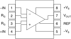
INA827 po_bos562.gif

Pin Functions

NAME NO. I/O DESCRIPTION
–IN 1 I Negative input
+IN 4 I Positive input
REF 6 I Reference input. This pin must be driven by low impedance.
RG 2, 3 Gain setting pin. Place a gain resistor between pin 2 and pin 3.
VOUT 7 O Output
–VS 5 Negative supply
+VS 8 Positive supply