JAJSOA9A March 2022 – October 2022 INA851
PRODUCTION DATA
- 1 特長
- 2 アプリケーション
- 3 説明
- 4 Revision History
- 5 Related Products
- 6 Pin Configuration and Functions
- 7 Specifications
- 8 Detailed Description
-
9 Application and Implementation
- 9.1 Application Information
- 9.2 Typical Applications
- 9.3 Power Supply Recommendations
- 9.4 Layout
- 10Device and Documentation Support
- 11Mechanical, Packaging, and Orderable Information
パッケージ・オプション
メカニカル・データ(パッケージ|ピン)
- RGT|16
サーマルパッド・メカニカル・データ
- RGT|16
発注情報
7.6 Typical Characteristics
at TA = 25°C, VS = ±15 V, VICM = VOCM = midsupply, VCLAMP+ = VS+, VCLAMP– = VS–, G = GIN = GOUT = 1 V/V, and RL = 10 kΩ (unless otherwise noted)
Table 7-1 Table of Graphs
| DESCRIPTION | FIGURE |
|---|---|
| Typical Distribution of Input Stage Offset Voltage | Figure 7-1 |
| Typical Distribution of Input Stage Offset Voltage Drift | Figure 7-2 |
| Typical Distribution of Output Stage Offset Voltage, G = 1 | Figure 7-3 |
| Typical Distribution of Output Stage Offset Voltage, G = 0.2 | Figure 7-4 |
| Typical Distribution of Output Stage Offset Voltage Drift | Figure 7-5 |
| Typical Distribution of Input Offset Current | Figure 7-6 |
| Typical Distribution of Input Bias Current, TA = 25°C | Figure 7-7 |
| Typical Distribution of Input Bias Current, TA = 90°C | Figure 7-8 |
| Typical CMRR Distribution, G = 1 | Figure 7-9 |
| Typical CMRR Distribution, G = 10 | Figure 7-10 |
| Typical Distribution of Gain Error, G = 0.2 | Figure 7-11 |
| Typical Distribution of Gain Error, G = 1 | Figure 7-12 |
| Typical Distribution of Gain Error, G = 10 | Figure 7-13 |
| Input Stage Offset Voltage vs Temperature | Figure 7-14 |
| Input Bias Current vs Temperature | Figure 7-15 |
| Input Offset Current vs Temperature | Figure 7-16 |
| Input-Referred Output Offset Voltage vs Temperature | Figure 7-17 |
| CMRR vs Temperature, G = 1 | Figure 7-18 |
| CMRR vs Temperature, G = 10 | Figure 7-19 |
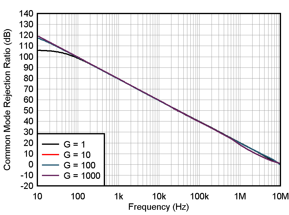
| CMRR vs Frequency (RTI) | Figure 7-20 |
| CMRR vs Frequency (RTI, 1-kΩ source imbalance) | Figure 7-21 |
| Positive/Negative PSRR vs Frequency (RTI) | Figure 7-22 |
| PSRR vs Frequency of VCLAMP+ (RTI) | Figure 7-23 |
| Gain vs Frequency | Figure 7-24 |
| Voltage Noise Spectral Density vs Frequency (RTI) | Figure 7-25 |
| Current Noise Spectral Density vs Frequency (RTI) | Figure 7-26 |
| 0.1-Hz to 10-Hz RTI Voltage Noise, G = 0.2 | Figure 7-27 |
| 0.1-Hz to 10-Hz RTI Voltage Noise, G = 1 | Figure 7-28 |
| 0.1-Hz to 10-Hz RTI Voltage Noise, G = 1000 | Figure 7-29 |
| Positive Input Bias Current vs Common-Mode Voltage | Figure 7-30 |
| Negative Input Bias Current vs Common-Mode Voltage | Figure 7-31 |
| Gain Error vs Temperature | Figure 7-32 |
| Quiescent Current vs Temperature | Figure 7-33 |
| Gain Nonlinearity, G = 1 | Figure 7-34 |
| Gain Nonlinearity, G = 10 | Figure 7-35 |
| Offset Voltage vs Negative Common-Mode Voltage | Figure 7-36 |
| Offset Voltage vs Positive Common-Mode Voltage | Figure 7-37 |
| Positive Output Voltage Swing vs Output Current | Figure 7-38 |
| Negative Output Voltage Swing vs Output Current | Figure 7-39 |
| Claw Curve of VCLAMP+ | Figure 7-40 |
| Short Circuit Current vs Temperature | Figure 7-41 |
| Large-Signal Frequency Response | Figure 7-42 |
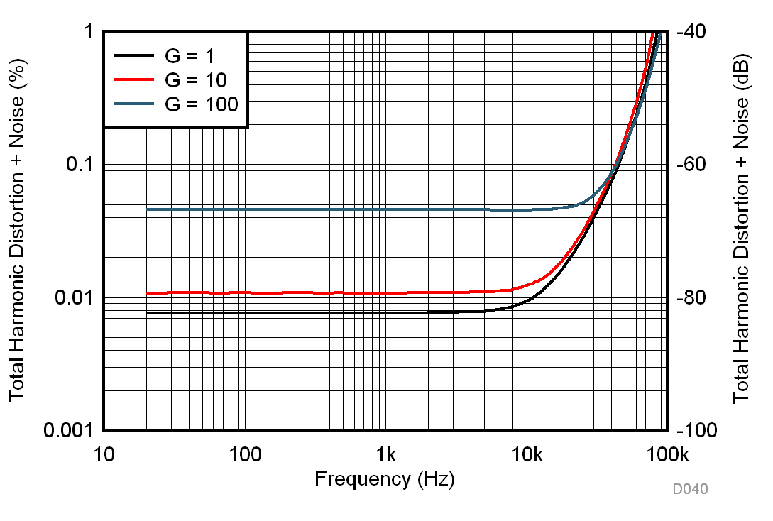
| THD+N vs Frequency | Figure 7-43 |
| Overshoot vs Capacitive Loads | Figure 7-44 |
| Small-Signal Response with different Output Capacitors G = 1 V/V | Figure 7-45 |
| Small-Signal Response, G = 0.2 | Figure 7-46 |
| Small-Signal Response, G = 1 | Figure 7-47 |
| Small-Signal Response, G = 10 | Figure 7-48 |
| Small-Signal Response, G = 1000 | Figure 7-49 |
| Small-Signal Response of VOCM Amplifier | Figure 7-50 |
| Large Signal Step Response | Figure 7-51 |
| Closed-Loop Output Impedance | Figure 7-52 |
| Settling Time for G = 0.2 | Figure 7-53 |
| Settling Time for G = 1 | Figure 7-54 |
| Offset Warm-up for G = 1 | Figure 7-55 |
| Offset Warm-up for G = 100 | Figure 7-56 |
| N = 150 | Mean = –2.32 µV | Std. Dev. = 6.73 µV |
Input Stage Offset Voltage
| N = 150 | Mean = –27.84 µV | Std. Dev. = 82.71 µV |
| G = 1 V/V |
| N = 82 | Mean = –4.98 µV/°C | Std. Dev. = 1.59 µV/°C |
| N = 107 | Mean = –2.34 nA | Std. Dev. = 0.78 nA |
| TA = 25°C |
| N = 150 | Mean = –4.78 µV/V | Std. Dev. = 8.67 µV/V |
| G = 1 V/V |
| N = 293 | Mean = –0.017% | Std. Dev. = 0.005% |
| N = 297 | Mean = –0.0048 % | Std. Dev. = 0.0136% |
| G = 10 V/V |
| N = 54 | ||
| N = 50 | ||
| G = 10 | ||

| 1-kΩ source imbalance | ||
| eN(RTI) = √[eNI2 + (eNO(G0.2 or G1) / GIN)2] |
| G = 0.2 V/V |
| G = 1000 V/V |
| G = 10 |

| 500-kHz measurement bandwidth | ||
| 1-VRMS output voltage | 100-kΩ load | |
| G = 1 | RL = 10 kΩ | |
| G = 1 V/V | RL = 10 kΩ | CL = 100 pF |
| G = 1000 V/V | RL = 10 kΩ | CL = 100 pF |
| G = 0.2 V/V | ||
| G = 1 V/V | ||
| N = 82 | Mean = 0.062 µV/°C | Std. Dev. = 0.0738 µV/°C |
| N = 150 | Mean = –97.17 μV | Std. Dev. = 179.33 μV |
| G = 0.2 V/V |
| N = 53 | Mean = –0.14 nA | Std. Dev. = 0.50 nA |
Input Offset Current
| N = 107 | Mean = –2.2 nA | Std. Dev. = 0.75 nA |
| TA = 90°C |
| N = 300 | Mean = –0.62 µV/V | Std. Dev. = 1.03 µV/V |
| G = 10 V/V |
| N = 293 | Mean = –0.0037% | Std. Dev. = 0.0011% |
| G = 1 V/V |
| N = 52 | ||
| N = 54 | ||
| G = 1000 V/V |
| G = 1 V/V |
| G = 1 |
| G = 0.2 V/V | RL = 10 kΩ | CL = 100 pF |
| G = 10 V/V | RL = 10 kΩ | CL = 100 pF |
| G = 1 V/V | ||
| G = 100 V/V | ||