JAJSDX8E June 2017 – August 2018 ISO1211 , ISO1212
PRODUCTION DATA.
- 1 特長
- 2 アプリケーション
- 3 概要
- 4 改訂履歴
- 5 概要(続き)
- 6 Pin Configuration and Functions
-
7 Specifications
- 7.1 Absolute Maximum Ratings
- 7.2 ESD Ratings
- 7.3 Recommended Operating Conditions
- 7.4 Thermal Information
- 7.5 Power Ratings
- 7.6 Insulation Specifications
- 7.7 Safety-Related Certifications
- 7.8 Safety Limiting Values
- 7.9 Electrical Characteristics—DC Specification
- 7.10 Switching Characteristics—AC Specification
- 7.11 Insulation Characteristics Curves
- 7.12 Typical Characteristics
- 8 Parameter Measurement Information
- 9 Detailed Description
-
10Application and Implementation
- 10.1 Application Information
- 10.2
Typical Application
- 10.2.1
Sinking Inputs
- 10.2.1.1 Design Requirements
- 10.2.1.2
Detailed Design Procedure
- 10.2.1.2.1 Setting Current Limit and Voltage Thresholds
- 10.2.1.2.2 Thermal Considerations
- 10.2.1.2.3 Designing for 48-V Systems
- 10.2.1.2.4 Designing for Input Voltages Greater Than 60 V
- 10.2.1.2.5 Surge, ESD, and EFT Tests
- 10.2.1.2.6 Multiplexing the Interface to the Host Controller
- 10.2.1.2.7 Status LEDs
- 10.2.1.3 Application Curve
- 10.2.2 Sourcing Inputs
- 10.2.3 Sourcing and Sinking Inputs (Bidirectional Inputs)
- 10.2.1
Sinking Inputs
- 11Power Supply Recommendations
- 12Layout
- 13デバイスおよびドキュメントのサポート
- 14メカニカル、パッケージ、および注文情報
パッケージ・オプション
デバイスごとのパッケージ図は、PDF版データシートをご参照ください。
メカニカル・データ(パッケージ|ピン)
- D|8
サーマルパッド・メカニカル・データ
発注情報
10.2.3 Sourcing and Sinking Inputs (Bidirectional Inputs)
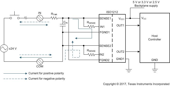
The ISO1212 device can be used to create a bidirectional input module that can sink and source current as shown in Figure 29. In this configuration, channel 1 is active if the COM terminal is connected to ground for sinking inputs, and channel 2 is active if the COM terminal is connected to 24 V for sourcing input. The digital input is considered high if either the OUT1 or OUT2 pin is high.
 Figure 29. Application Circuit—ISO1212 With Sourcing and Sinking Inputs
 A bidirectional input module can also be built with the ISO121x devices using low-cost Schottky diodes as shown in Figure 30.
 Figure 30. Bidirectional Implementation With ISO1211 and Bridge Rectifier