JAJSDX8E June 2017 – August 2018 ISO1211 , ISO1212
PRODUCTION DATA.
- 1 特長
- 2 アプリケーション
- 3 概要
- 4 改訂履歴
- 5 概要(続き)
- 6 Pin Configuration and Functions
-
7 Specifications
- 7.1 Absolute Maximum Ratings
- 7.2 ESD Ratings
- 7.3 Recommended Operating Conditions
- 7.4 Thermal Information
- 7.5 Power Ratings
- 7.6 Insulation Specifications
- 7.7 Safety-Related Certifications
- 7.8 Safety Limiting Values
- 7.9 Electrical Characteristics—DC Specification
- 7.10 Switching Characteristics—AC Specification
- 7.11 Insulation Characteristics Curves
- 7.12 Typical Characteristics
- 8 Parameter Measurement Information
- 9 Detailed Description
-
10Application and Implementation
- 10.1 Application Information
- 10.2
Typical Application
- 10.2.1
Sinking Inputs
- 10.2.1.1 Design Requirements
- 10.2.1.2
Detailed Design Procedure
- 10.2.1.2.1 Setting Current Limit and Voltage Thresholds
- 10.2.1.2.2 Thermal Considerations
- 10.2.1.2.3 Designing for 48-V Systems
- 10.2.1.2.4 Designing for Input Voltages Greater Than 60 V
- 10.2.1.2.5 Surge, ESD, and EFT Tests
- 10.2.1.2.6 Multiplexing the Interface to the Host Controller
- 10.2.1.2.7 Status LEDs
- 10.2.1.3 Application Curve
- 10.2.2 Sourcing Inputs
- 10.2.3 Sourcing and Sinking Inputs (Bidirectional Inputs)
- 10.2.1
Sinking Inputs
- 11Power Supply Recommendations
- 12Layout
- 13デバイスおよびドキュメントのサポート
- 14メカニカル、パッケージ、および注文情報
パッケージ・オプション
デバイスごとのパッケージ図は、PDF版データシートをご参照ください。
メカニカル・データ(パッケージ|ピン)
- DBQ|16
サーマルパッド・メカニカル・データ
発注情報
10.2.1.2.1 Setting Current Limit and Voltage Thresholds
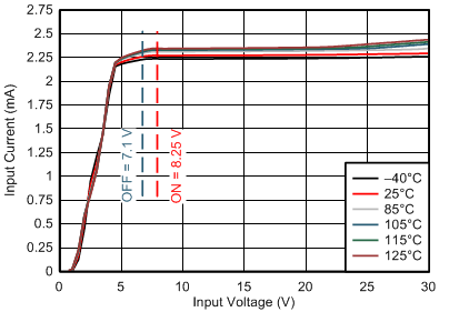
The RSENSE resistor limits the current drawn from the field input. A value of 562 Ω for RSENSE is recommended for Type 1 and Type 3 operation, and results in a current limit of 2.25 mA (typical). A value of 200 Ω for RSENSE is recommended for Type 2 operation, and results in a current limit of 6 mA (typical). In each case, a (slightly) lower value of RSENSE can be selected based on the need for a higher current limit or component availability. For more information, see the Electrical Characteristics—DC Specification table and Typical Characteristics section. A 1% tolerance is recommended on RSENSE but 5% resistors can also be used if higher variation in the current limit value is acceptable. The relationship between the RSENSE resistor and the typical current limit (IL) is given by Equation 1.

The RTHR resistor sets the voltage thresholds (VIL and VIH) as well as limits the surge current. A value of 1 kΩ is recommended for RTHR in Type 3 systems (maximum threshold voltage required is 11 V). A value of 2.5 kΩ is recommended for RTHR in Type 1 systems (maximum threshold voltage required is 15 V) and a value of 330 Ω is recommended for RTHR in Type 2 systems. The Electrical Characteristics—DC Specification table lists and the Typical Characteristics section describes the voltage thresholds with different values of RTHR. For other values of RTHR, derive the values through linear interpolation. Use Equation 2 and Equation 3 to calculate the values for the typical VIH values and minimum VIL values, respectively.

The maximum voltage on the SENSE pins of the ISO121x device is 60 V. However, because the RTHR resistor drops additional voltage, the maximum voltage supported at the module inputs is higher and given by Equation 4.

Use the ISO121x Threshold Calculator for 9V to 300V DC and AC Voltage Detection to estimate the values of the voltage transition thresholds, the maximum-allowed module input voltage, and module input current for the given values of the RSENSE and RTHR resistors.
A value of 0 Ω for RTHR also meets Type 1, Type 2 and Type 3 voltage-threshold requirements. The value of RTHR should be maximized for best EMC performance while meeting the desired input voltage thresholds. Because RTHR is used to limit surge current, 0.25 W MELF resistors must be used.
Figure 18 shows the typical input current characteristics and voltage transition thresholds for 562-Ω RSENSE and 1-kΩ RTHR.
 Figure 18. Transition Thresholds