JAJSQF6D june 2015 – may 2023 ISO5451
PRODUCTION DATA
- 1
- 1 特長
- 2 アプリケーション
- 3 説明
- 4 Revision History
- 5 概要 (続き)
- 6 Pin Configuration and Function
-
7 Specifications
- 7.1 Absolute Maximum Ratings
- 7.2 ESD Ratings
- 7.3 Recommended Operating Conditions
- 7.4 Thermal Information
- 7.5 Power Ratings
- 7.6 Insulation Characteristics
- 7.7 Safety-Related Certifications
- 7.8 Safety Limiting Values
- 7.9 Electrical Characteristics
- 7.10 Switching Characteristics
- 7.11 Insulation Characteristics Curves
- 7.12 Typical Characteristics
- 8 Parameter Measurement Information
- 9 Detailed Description
-
10Application and Implementation
- 10.1 Application Information
- 10.2
Typical Applications
- 10.2.1 Design Requirements
- 10.2.2
Detailed Design Procedure
- 10.2.2.1 Recommended ISO5451 Application Circuit
- 10.2.2.2 FLT and RDY Pin Circuitry
- 10.2.2.3 Driving the Control Inputs
- 10.2.2.4 Local Shutdown and Reset
- 10.2.2.5 Global-Shutdown and Reset
- 10.2.2.6 Auto-Reset
- 10.2.2.7 DESAT Pin Protection
- 10.2.2.8 DESAT Diode and DESAT Threshold
- 10.2.2.9 Determining the Maximum Available, Dynamic Output Power, POD-max
- 10.2.2.10 Example
- 10.2.2.11 Higher Output Current Using an External Current Buffer
- 10.2.3 Application Curves
- 11Power Supply Recommendations
- 12Layout
- 13Device and Documentation Support
- 14Mechanical, Packaging, and Orderable Information
パッケージ・オプション
デバイスごとのパッケージ図は、PDF版データシートをご参照ください。
メカニカル・データ(パッケージ|ピン)
- DW|16
サーマルパッド・メカニカル・データ
発注情報
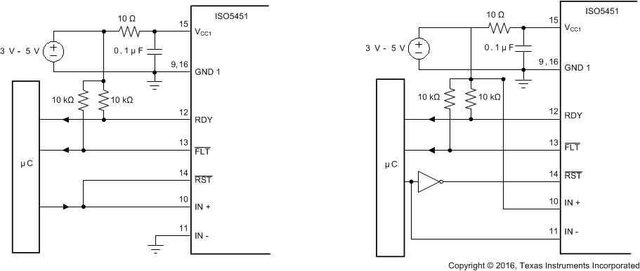
10.2.2.6 Auto-Reset
In this case, the gate control signal at IN+ is also applied to the RST input to reset the fault latch every switching cycle. Incorrect RST makes output go low. A fault condition, however, the gate driver remains in the latched fault state until the gate control signal changes to the gate low state and resets the fault latch.
If the gate control signal is a continuous PWM signal, the fault latch will always be reset before IN+ goes high again. This configuration protects the IGBT on a cycle by cycle basis and automatically resets before the next 'on' cycle.
 Figure 10-7 Auto Reset for Noninverting and Inverting Input Configuration