JAJSJQ3E August   2021  – February 2023 ISO6760 , ISO6761 , ISO6762 , ISO6763

PRODUCTION DATA  

  1. 特長
  2. アプリケーション
  3. 概要
  4. Revision History
  5. Pin Configuration and Functions
  6. Specifications
    1. 6.1  Absolute Maximum Ratings
    2. 6.2  ESD Ratings
    3. 6.3  Recommended Operating Conditions
    4. 6.4  Thermal Information
    5. 6.5  Power Ratings
    6. 6.6  Insulation Specifications
    7. 6.7  Safety-Related Certifications
    8. 6.8  Safety Limiting Values
    9. 6.9  Electrical Characteristics—5-V Supply
    10. 6.10 Supply Current Characteristics—5-V Supply
    11. 6.11 Electrical Characteristics—3.3-V Supply
    12. 6.12 Supply Current Characteristics—3.3-V Supply
    13. 6.13 Electrical Characteristics—2.5-V Supply 
    14. 6.14 Supply Current Characteristics—2.5-V Supply
    15. 6.15 Electrical Characteristics—1.8-V Supply
    16. 6.16 Supply Current Characteristics—1.8-V Supply
    17. 6.17 Switching Characteristics—5-V Supply
    18. 6.18 Switching Characteristics—3.3-V Supply
    19. 6.19 Switching Characteristics—2.5-V Supply
    20. 6.20 Switching Characteristics—1.8-V Supply
    21. 6.21 絶縁特性曲線
    22. 6.22 Typical Characteristics
  7. Parameter Measurement Information
  8. Detailed Description
    1. 8.1 Overview
    2. 8.2 Functional Block Diagram
    3. 8.3 Feature Description
      1. 8.3.1 Electromagnetic Compatibility (EMC) Considerations
    4. 8.4 Device Functional Modes
      1. 8.4.1 Device I/O Schematics
  9. Application and Implementation
    1. 9.1 Application Information
    2. 9.2 Typical Application
      1. 9.2.1 Design Requirements
      2. 9.2.2 Detailed Design Procedure
      3. 9.2.3 Application Curve
        1. 9.2.3.1 Insulation Lifetime
  10. 10Power Supply Recommendations
  11. 11Layout
    1. 11.1 Layout Guidelines
      1. 11.1.1 PCB Material
    2. 11.2 Layout Example
  12. 12Device and Documentation Support
    1. 12.1 Documentation Support
      1. 12.1.1 Related Documentation
    2. 12.2 Receiving Notification of Documentation Updates
    3. 12.3 サポート・リソース
    4. 12.4 Trademarks
    5. 12.5 静電気放電に関する注意事項
    6. 12.6 用語集
  13. 13Mechanical, Packaging, and Orderable Information

パッケージ・オプション

メカニカル・データ(パッケージ|ピン)
サーマルパッド・メカニカル・データ
発注情報

Typical Characteristics

GUID-20211116-SS0I-SGXH-7HZB-LVLJFSCKTSGX-low.svg
TA = 25°C CL = 15 pF
Figure 6-3 ISO6760 Supply Current vs Data Rate (With 15-pF Load)
GUID-20211116-SS0I-BDWS-ZWJJ-8RW14WZPBM1L-low.svg
TA = 25°C CL = 15 pF
Figure 6-5 ISO6761 Supply Current vs Data Rate (With 15-pF Load)
GUID-20211116-SS0I-B0PT-K8WQ-X8RMFMBVXVS7-low.svg
TA = 25°C CL = 15 pF
Figure 6-7 ISO6762 Supply Current vs Data Rate (With 15-pF Load)
GUID-20210818-SS0I-M1LM-92NJ-FPNCCSVRBKHK-low.gif
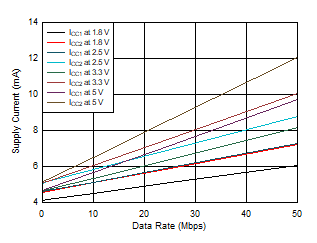
TA = 25°C CL = 15 pF
Figure 6-9 ISO6763 Supply Current vs Data Rate (With 15-pF Load)
GUID-20201201-CA0I-NWPL-PH2L-F8QFFQVHKN17-low.gif
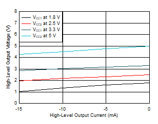
TA = 25°C
Figure 6-11 High-Level Output Voltage vs High-level Output Current
GUID-20201201-CA0I-0L80-FXT4-TWK5WLVFDNQ6-low.gif
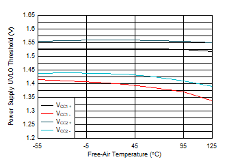
Figure 6-13 Power Supply Undervoltage Threshold vs Free-Air Temperature
GUID-20211116-SS0I-J6SB-ZF6V-ZJSCMPJJM3FC-low.svg
TA = 25°C CL = No Load
Figure 6-4 ISO6760 Supply Current vs Data Rate (With No Load)
GUID-20211116-SS0I-KCWB-0GCV-ZRQLQF1FDGNR-low.svg
TA = 25°C CL = No Load
Figure 6-6 ISO6761 Supply Current vs Data Rate (With No Load)
GUID-20211116-SS0I-VKRM-3MZT-SB11W1BGFCZS-low.svg
TA = 25°C CL = No Load
Figure 6-8 ISO6762 Supply Current vs Data Rate (With No Load)
GUID-20210818-SS0I-CSSG-KDDF-DSNDCWVTKBXP-low.svg
TA = 25°C CL = No Load
Figure 6-10 ISO6763 Supply Current vs Data Rate (With No Load)
GUID-20210818-SS0I-43MF-RLR4-WQXQKSQJSG6P-low.gif
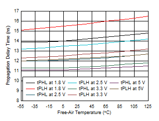
Figure 6-12 Propagation Delay Time vs Free-Air Temperature
GUID-20201201-CA0I-HDJZ-BWKX-ZHSKPJLRFK3F-low.svg
TA = 25°C
Figure 6-14 Low-Level Output Voltage vs Low-Level Output Current