JAJSVN0E July 2009 – November 2024 ISO7220A-Q1 , ISO7221A-Q1 , ISO7221C-Q1
PRODUCTION DATA
- 1
- 1 特長
- 2 アプリケーション
- 3 概要
- 4 Pin Configuration and Functions
-
5 Specifications
- 5.1 Absolute Maximum Ratings
- 5.2 Recommended Operating Conditions
- 5.3 Safety-Related Certifications
- 5.4 Thermal Information
- 5.5 Safety Limiting Values
- 5.6 Insulation Specifications
- 5.7 Electrical Characterstics
- 5.8 Electrical Characteristics
- 5.9 Electrical Characteristics
- 5.10 Electrical Charcteristics
- 5.11 Switching Characteristics
- 5.12 Switching Characteristics
- 5.13 Switching Characteristics
- 5.14 Switching Characteristics
- 5.15 Typical Characteristics
- 6 Parameter Measurement Information
- 7 Detailed Description
- 8 Application and Implementation
- 9 Device and Documentation Support
- 10Revision History
- 11Mechanical, Packaging, and Orderable Information
5.15 Typical Characteristics
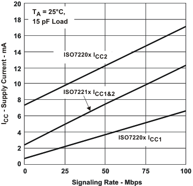 Figure 5-1 3.3-V RMS Supply Current vs Signaling Rate
(Mbps)
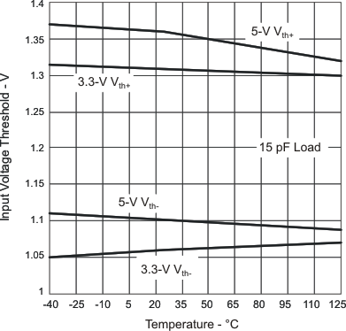 Figure 5-3 ISO722xA-Q1 and ISO722xC -Q1 Input Voltage
Low-to-High Switching Threshold vs Free-Air
Temperature
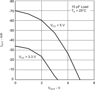 Figure 5-5 High-Level Output Current vs High-Level Output
Voltage
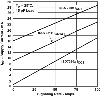 Figure 5-2 5-V RMS Suppply Current vs Signaling Rate
(Mbps)
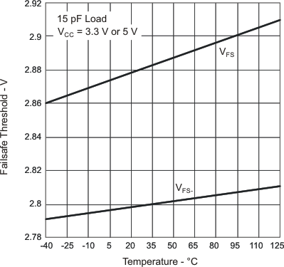 Figure 5-4 VCC Failsafe Threshold vs Free-Air
Temperature
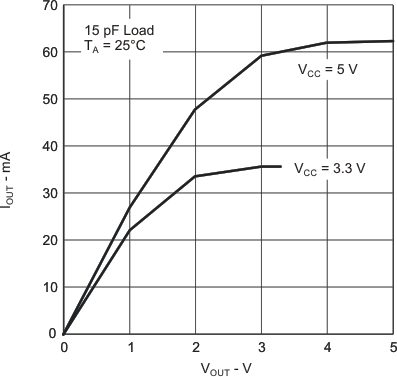 Figure 5-6 Low-Level Output Current vs Low-Level Output
Voltage