JAJSVN0E July 2009 – November 2024 ISO7220A-Q1 , ISO7221A-Q1 , ISO7221C-Q1
PRODUCTION DATA
- 1
- 1 特長
- 2 アプリケーション
- 3 概要
- 4 Pin Configuration and Functions
-
5 Specifications
- 5.1 Absolute Maximum Ratings
- 5.2 Recommended Operating Conditions
- 5.3 Safety-Related Certifications
- 5.4 Thermal Information
- 5.5 Safety Limiting Values
- 5.6 Insulation Specifications
- 5.7 Electrical Characterstics
- 5.8 Electrical Characteristics
- 5.9 Electrical Characteristics
- 5.10 Electrical Charcteristics
- 5.11 Switching Characteristics
- 5.12 Switching Characteristics
- 5.13 Switching Characteristics
- 5.14 Switching Characteristics
- 5.15 Typical Characteristics
- 6 Parameter Measurement Information
- 7 Detailed Description
- 8 Application and Implementation
- 9 Device and Documentation Support
- 10Revision History
- 11Mechanical, Packaging, and Orderable Information
7.4 Device Functional Modes
The ISO7220x-Q1 and ISO7221x-Q1 family of devices functional modes are listed in Table 7-2.
Table 7-2 ISO7220x-Q1 or ISO7221x-Q1 Function
Table
| INPUT SIDE VCC(1) | OUTPUT SIDE VCC | INPUT (IN) | OUTPUT (OUT) |
|---|---|---|---|
| PU | PU | H | H |
| L | L | ||
| Open | H | ||
| PD | PU | X | H |
| X | PD | X | Undetermined |
(1) PU = Powered Up (VCC ≥ 3.0 V), PD = Powered Down (VCC ≤ 2.5 V), X = Irrelevant, H = High Level,
L = Low Level
L = Low Level
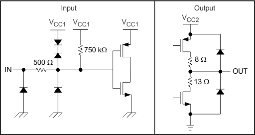
 Figure 7-1 Device I/O Schematics