SLLSEN3 December 2015 ISO7421-EP
PRODUCTION DATA.
- 1 Features
- 2 Applications
- 3 Description
- 4 Revision History
- 5 Pin Configuration and Functions
-
6 Specifications
- 6.1 Absolute Maximum Ratings
- 6.2 ESD Ratings
- 6.3 Recommended Operating Conditions
- 6.4 Thermal Information
- 6.5 Electrical Characteristics: VCC1 and VCC2 at 5 V ±10%
- 6.6 Electrical Characteristics: VCC1 at 5 V ±10%, VCC2 at 3.3 V ±10%
- 6.7 Electrical Characteristics: VCC1 at 3.3 V ±10%, VCC2 at 5 V ±10%
- 6.8 Electrical Characteristics: VCC1 and VCC2 at 3.3 V ±10%
- 6.9 Power Dissipation
- 6.10 Switching Characteristics: VCC1 and VCC2 at 5 V ±10%
- 6.11 Switching Characteristics: VCC1 at 5 V ±10%, VCC2 at 3.3 V ±10%
- 6.12 Switching Characteristics: VCC1 at 3.3 V ±10%, VCC2 at 5 V ±10%
- 6.13 Switching Characteristics: VCC1 and VCC2 at 3.3 V ±10%
- 6.14 Typical Characteristics
- 7 Parameter Measurement Information
- 8 Detailed Description
- 9 Application and Implementation
- 10Power Supply Recommendations
- 11Layout
- 12Device and Documentation Support
- 13Mechanical, Packaging, and Orderable Information
9 Application and Implementation
NOTE
Information in the following applications sections is not part of the TI component specification, and TI does not warrant its accuracy or completeness. TI’s customers are responsible for determining suitability of components for their purposes. Customers should validate and test their design implementation to confirm system functionality.
9.1 Application Information
The ISO7421-EP device uses a single-ended TTL-logic switching technology. Its supply voltage range is from 3.15 V to 5.25 V for both supplies, VCC1 and VCC2. When designing with digital isolators, it is important to keep in mind that due to the single-ended design structure, digital isolators do not conform to any specific interface standard and are only intended for isolating single-ended CMOS or TTL digital signal lines. The isolator is typically placed between the data controller (that is, μC or UART), and a data converter or a line transceiver, regardless of the interface type or standard.
9.2 Typical Application
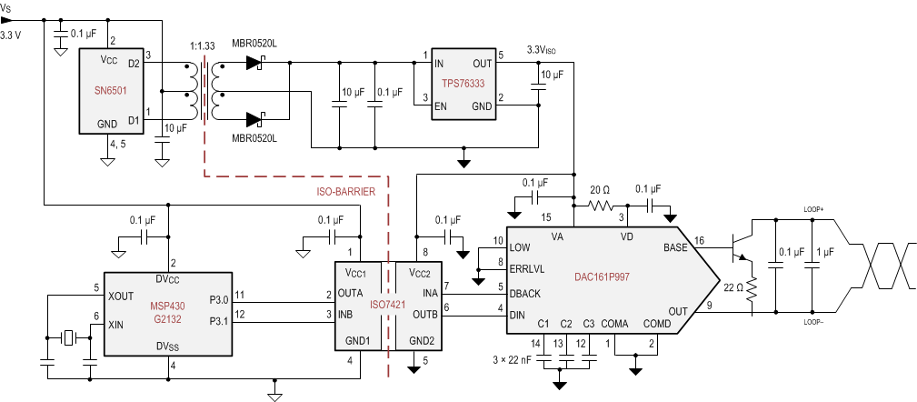
ISO7421-EP can be used with Texas Instruments' mixed signal micro-controller, digital-to-analog converter, transformer driver, and voltage regulator to create an isolated 4-20 mA current loop.
 Figure 12. Isolated 4- to 20-mA Current Loop
9.2.1 Design Requirements
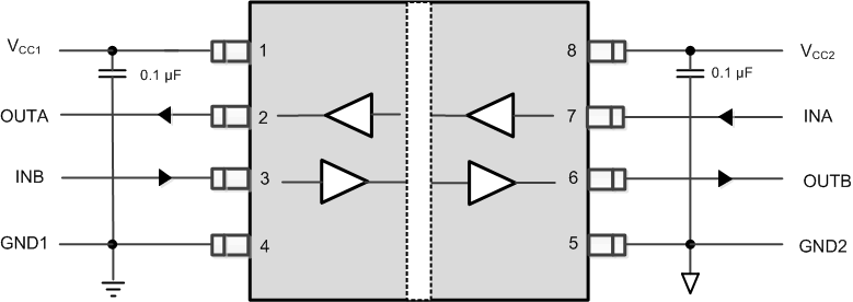
For applications that require isolation in place of using x-fmr to provide isolation, ISO7421-EP meets the system needs with small size. Unlike optocouplers, which require external components to improve performance, provide bias, or limit current, the ISO7421-EP device only requires two external bypass capacitors to operate.
9.2.2 Detailed Design Procedure
ISO7421 digital isolator containing two channels has logic input and output buffer isolated by silicon dioxide (SiO2) isolation barrier. When using ISO7421 in conjunction with isolated power supplies, these devices prevent noise currents on a data bus or other circuit from entering the local ground and interfering with or damaging sensitive circuitry. ISO7421 are specified for signaling rate up to 1Mbps. These devices also transmit data with much shorter pulse widths, in most cases, because of their fast response time. Designer must add external filtering to remove spurious signals with input pulse duration < 20 ns.
 Figure 13. Typical ISO7421-EP Circuit Hookup
9.2.3 Application Curve
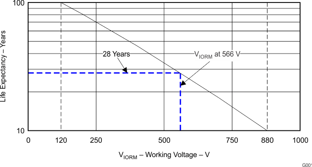
 Figure 14. Life Expectancy vs Working Voltage