SLLSEN3 December 2015 ISO7421-EP
PRODUCTION DATA.
- 1 Features
- 2 Applications
- 3 Description
- 4 Revision History
- 5 Pin Configuration and Functions
-
6 Specifications
- 6.1 Absolute Maximum Ratings
- 6.2 ESD Ratings
- 6.3 Recommended Operating Conditions
- 6.4 Thermal Information
- 6.5 Electrical Characteristics: VCC1 and VCC2 at 5 V ±10%
- 6.6 Electrical Characteristics: VCC1 at 5 V ±10%, VCC2 at 3.3 V ±10%
- 6.7 Electrical Characteristics: VCC1 at 3.3 V ±10%, VCC2 at 5 V ±10%
- 6.8 Electrical Characteristics: VCC1 and VCC2 at 3.3 V ±10%
- 6.9 Power Dissipation
- 6.10 Switching Characteristics: VCC1 and VCC2 at 5 V ±10%
- 6.11 Switching Characteristics: VCC1 at 5 V ±10%, VCC2 at 3.3 V ±10%
- 6.12 Switching Characteristics: VCC1 at 3.3 V ±10%, VCC2 at 5 V ±10%
- 6.13 Switching Characteristics: VCC1 and VCC2 at 3.3 V ±10%
- 6.14 Typical Characteristics
- 7 Parameter Measurement Information
- 8 Detailed Description
- 9 Application and Implementation
- 10Power Supply Recommendations
- 11Layout
- 12Device and Documentation Support
- 13Mechanical, Packaging, and Orderable Information
11 Layout
11.1 Layout Guidelines
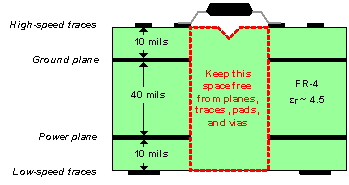
There are several signals that conduct fast charging current or voltages that can interact with stray inductance or parasitic capacitors to generate noise. Thus to eliminate these problems Vin ins of ISO7421 should be bypass to gnd with low esr ceramic bypass capacitor with X7R dielectric. A minimum of four layers is required to accomplish a low EMI PCB design (see Figure 15). Layer stacking should be in the following order (top-to-bottom): high-speed signal layer, ground plane, power plane and low-frequency signal layer.
- Routing the high-speed traces on the top layer avoids the use of vias (and the introduction of their inductances) and allows for clean interconnects between the isolator and the transmitter and receiver circuits of the data link.
- Placing a solid ground plane next to the high-speed signal layer establishes controlled impedance for transmission line interconnects and provides an excellent low-inductance path for the return current flow.
- Placing the power plane next to the ground plane creates additional high-frequency bypass capacitance of approximately 100pF/in2.
- Routing the slower speed control signals on the bottom layer allows for greater flexibility as these signal links usually have margin to tolerate discontinuities such as vias.
If an additional supply voltage plane or signal layer is needed, add a second power / ground plane system to the stack to keep it symmetrical. This makes the stack mechanically stable and prevents it from warping. Also the power and ground plane of each power system can be placed closer together, thus increasing the high-frequency bypass capacitance significantly.
For detailed layout recommendations, see Application Note Digital Isolator Design Guide, SLLA284.
11.1.1 PCB Material
For digital circuit boards operating below 150 Mbps, (or rise and fall times higher than 1 ns), and trace lengths of up to 10 inches, use standard FR-4 epoxy-glass as PCB material. FR-4 (Flame Retardant 4) meets the requirements of Underwriters Laboratories UL94-V0, and is preferred over cheaper alternatives due to its lower dielectric losses at high frequencies, less moisture absorption, greater strength and stiffness, and its self-extinguishing flammability-characteristics.
11.2 Layout Example
 Figure 15. Recommended Layer Stack