SLLSEP8B July 2015 – June 2016 ISO7831
PRODUCTION DATA.
- 1 Features
- 2 Applications
- 3 Description
- 4 Revision History
- 5 Pin Configuration and Functions
-
6 Specifications
- 6.1 Absolute Maximum Ratings
- 6.2 ESD Ratings
- 6.3 Recommended Operating Conditions
- 6.4 Thermal Information
- 6.5 Power Rating
- 6.6 Insulation Characteristics
- 6.7 Regulatory Information
- 6.8 Safety Limiting Values
- 6.9 Electrical Characteristics—5-V Supply
- 6.10 Supply Current Characteristics—5-V Supply
- 6.11 Electrical Characteristics—3.3-V Supply
- 6.12 Supply Current Characteristics—3.3-V Supply
- 6.13 Electrical Characteristics—2.5-V Supply
- 6.14 Supply Current Characteristics—2.5-V Supply
- 6.15 Switching Characteristics—5-V Supply
- 6.16 Switching Characteristics—3.3-V Supply
- 6.17 Switching Characteristics—2.5-V Supply
- 6.18 Insulation Characteristics Curves
- 6.19 Typical Characteristics
- 7 Parameter Measurement Information
- 8 Detailed Description
- 9 Application and Implementation
- 10Power Supply Recommendations
- 11Layout
- 12Device and Documentation Support
- 13Mechanical, Packaging, and Orderable Information
パッケージ・オプション
デバイスごとのパッケージ図は、PDF版データシートをご参照ください。
メカニカル・データ(パッケージ|ピン)
- DWW|16
- DW|16
サーマルパッド・メカニカル・データ
発注情報
8 Detailed Description
8.1 Overview
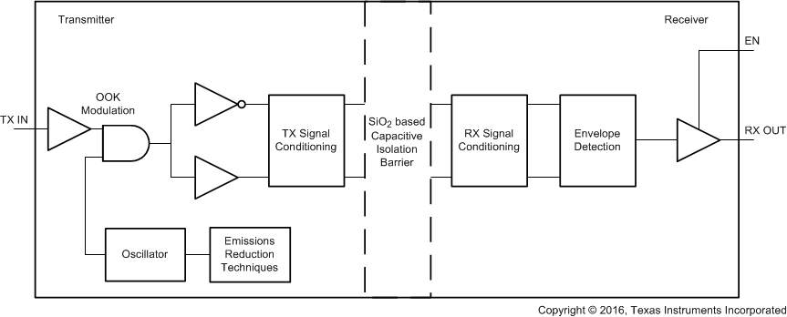
The ISO7831x device has an ON-OFF keying (OOK) modulation scheme to transmit the digital data across a silicon dioxide based isolation barrier. The transmitter sends a high frequency carrier across the barrier to represent one digital state and sends no signal to represent the other digital state. The receiver demodulates the signal after advanced signal conditioning and produces the output through a buffer stage. If the EN pin is low then the output goes to high impedance. The ISO7831x device also incorporates advanced circuit techniques to maximize the CMTI performance and minimize the radiated emissions because of the high frequency carrier and IO buffer switching. The conceptual block diagram of a digital capacitive isolator, Figure 17, shows a functional block diagram of a typical channel.
8.2 Functional Block Diagram
 Figure 17. Conceptual Block Diagram of a Digital Capacitive Isolator
Figure 18 shows a conceptual detail of how the ON-OFF keying scheme works.
 Figure 18. On-Off Keying (OOK) Based Modulation Scheme
8.3 Feature Description
Table 1 provides an overview of the device features.
Table 1. Device Features
| PART NUMBER | CHANNEL DIRECTION | RATED ISOLATION | MAXIMUM DATA RATE | DEFAULT OUTPUT |
|---|---|---|---|---|
| ISO7831 | 2 Forward, 1 Reverse
|
5700 VRMS / 8000 VPK(1) | 100 Mbps | High |
| ISO7831F | 2 Forward, 1 Reverse
|
5700 VRMS / 8000 VPK(1) | 100 Mbps | Low |
8.3.1 Electromagnetic Compatibility (EMC) Considerations
Many applications in harsh industrial environment are sensitive to disturbances such as electrostatic discharge (ESD), electrical fast transient (EFT), surge and electromagnetic emissions. These electromagnetic disturbances are regulated by international standards such as IEC 61000-4-x and CISPR 22. Although system-level performance and reliability depends, to a large extent, on the application board design and layout, the ISO7831x device incorporates many chip-level design improvements for overall system robustness. Some of these improvements include:
- Robust ESD protection cells for input and output signal pins and inter-chip bond pads.
- Low-resistance connectivity of ESD cells to supply and ground pins.
- Enhanced performance of high voltage isolation capacitor for better tolerance of ESD, EFT and surge events.
- Bigger on-chip decoupling capacitors to bypass undesirable high energy signals through a low impedance path.
- PMOS and NMOS devices isolated from each other by using guard rings to avoid triggering of parasitic SCRs.
- Reduced common mode currents across the isolation barrier by ensuring purely differential internal operation.
8.4 Device Functional Modes
Table 2 lists the ISO7831x functional modes.
Table 2. Function Table(1)
| VCCI | VCCO | INPUT (INx)(3) |
OUTPUT ENABLE (ENx) |
OUTPUT (OUTx) |
COMMENTS |
|---|---|---|---|---|---|
| PU | PU | H | H or open | H | Normal Operation: A channel output assumes the logic state of the input. |
| L | H or open | L | |||
| Open | H or open | Default | Default mode: When INx is open, the corresponding channel output goes to its default logic state. Default is High for ISO7831 and Low for ISO7831F. | ||
| X | PU | X | L | Z | A low value of output enable causes the outputs to be high-impedance |
| PD | PU | X | H or open | Default | Default mode: When VCCI is unpowered, a channel output assumes the logic state based on the selected default option. Default is High for ISO7831 and Low for ISO7831F.
When VCCI transitions from unpowered to powered-up, a channel output assumes the logic state of the input. When VCCI transitions from powered-up to unpowered, channel output assumes the selected default state. |
| X | PD | X | X | Undetermined | When VCCO is unpowered, a channel output state is undetermined (2). When VCCO transitions from unpowered to powered-up, a channel output assumes the logic state of the input |
8.4.1 Device I/O Schematics
 Figure 19. Device I/O Schematics