JAJSU29 March 2024 ISOUSB211-Q1
ADVANCE INFORMATION
- 1
- 1 特長
- 2 アプリケーション
- 3 概要
- 4 Pin Configuration and Functions
-
5 Specifications
- 5.1 Absolute Maximum Ratings
- 5.2 ESD Ratings
- 5.3 Recommended Operating Conditions
- 5.4 Thermal Information
- 5.5 Power Ratings
- 5.6 Insulation Specifications
- 5.7 Safety-Related Certifications
- 5.8 Safety Limiting Values
- 5.9 Electrical Characteristics
- 5.10 Switching Characteristics
- 5.11 Insulation Characteristics Curves
- 5.12 Typical Characteristics
- 6 Parameter Measurement Information
-
7 Detailed Description
- 7.1 Overview
- 7.2 Functional Block Diagram
- 7.3
Feature Description
- 7.3.1 Power Supply Options
- 7.3.2 Power Up
- 7.3.3 Symmetric Operation, Dual-Role Port and Role-Reversal
- 7.3.4 Connect and Speed Detection
- 7.3.5 Disconnect Detection
- 7.3.6 Reset
- 7.3.7 LS/FS Message Traffic
- 7.3.8 HS Message Traffic
- 7.3.9 Equalization and Pre-emphasis
- 7.3.10 L2 Power Management State (Suspend) and Resume
- 7.3.11 L1 Power Management State (Sleep) and Resume
- 7.3.12 HS Test Mode Support
- 7.3.13 CDP Advertising
- 7.4 Device Functional Modes
- 8 Application and Implementation
- 9 Device and Documentation Support
- 10Revision History
- 11Mechanical, Packaging, and Orderable Information
7.2 Functional Block Diagram
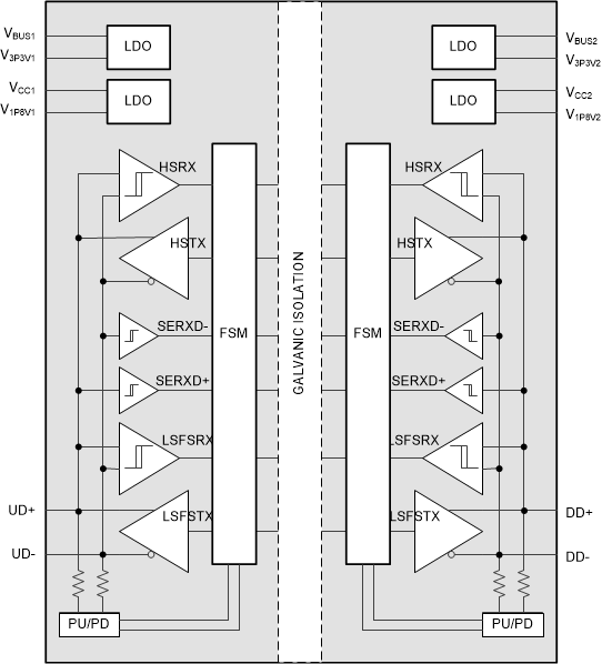
A simplified functional block diagram of ISOUSB211-Q1 is shown in Figure 7-1. The device comprises the following:  Figure 7-1 ISOUSB211-Q1 Simplified Functional Block Diagram.
- Transmit and receive circuits and pull-up and pull-down resistors according to the USB standard.
- Digital logic to handle bi-directional communication, and various state-transitions.
- Internal LDOs to generate V3P3Vxand V1P8Vxsupplies from the VBUSxand VCCxsupplies respectively.
- Galvanic isolation.
 Figure 7-1 ISOUSB211-Q1 Simplified Functional Block Diagram.