JAJSE44B May   2017  – April 2018 IWR1642

PRODUCTION DATA.  

  1. デバイスの概要
    1. 1.1 特長
    2. 1.2 アプリケーション
    3. 1.3 概要
    4. 1.4 機能ブロック図
  2. 改訂履歴
  3. Device Comparison
    1. 3.1 Related Products
  4. Terminal Configuration and Functions
    1. 4.1 Pin Diagram
    2. 4.2 Pin Attributes
      1. Table 4-3 PAD IO Register Bit Descriptions
    3. 4.3 Signal Descriptions
      1. Table 4-4 Signal Descriptions - Digital
      2. Table 4-5 Signal Descriptions - Analog
    4. 4.4 Pin Multiplexing
  5. Specifications
    1. 5.1  Absolute Maximum Ratings
    2. 5.2  ESD Ratings
    3. 5.3  Power-On Hours (POH)
    4. 5.4  Recommended Operating Conditions
    5. 5.5  Power Supply Specifications
    6. 5.6  Power Consumption Summary
    7. 5.7  RF Specification
    8. 5.8  CPU Specifications
    9. 5.9  Thermal Resistance Characteristics for FCBGA Package [ABL0161]
    10. 5.10 Timing and Switching Characteristics
      1. 5.10.1  Power Supply Sequencing and Reset Timing
      2. 5.10.2  Input Clocks and Oscillators
        1. 5.10.2.1 Clock Specifications
      3. 5.10.3  Multibuffered / Standard Serial Peripheral Interface (MibSPI)
        1. 5.10.3.1 Peripheral Description
        2. 5.10.3.2 MibSPI Transmit and Receive RAM Organization
          1. Table 5-7  SPI Timing Conditions
          2. Table 5-8  SPI Master Mode Switching Parameters (CLOCK PHASE = 0, SPICLK = output, SPISIMO = output, and SPISOMI = input)
          3. Table 5-9  SPI Master Mode Input Timing Requirements (CLOCK PHASE = 0, SPICLK = output, SPISIMO = output, and SPISOMI = input)
          4. Table 5-10 SPI Master Mode Switching Parameters (CLOCK PHASE = 1, SPICLK = output, SPISIMO = output, and SPISOMI = input)
          5. Table 5-11 SPI Master Mode Input Requirements (CLOCK PHASE = 1, SPICLK = output, SPISIMO = output, and SPISOMI = input)
        3. 5.10.3.3 SPI Slave Mode I/O Timings
          1. Table 5-12 SPI Slave Mode Switching Parameters (SPICLK = input, SPISIMO = input, and SPISOMI = output)
          2. Table 5-13 SPI Slave Mode Timing Requirements (SPICLK = input, SPISIMO = input, and SPISOMI = output)
        4. 5.10.3.4 Typical Interface Protocol Diagram (Slave Mode)
      4. 5.10.4  LVDS Interface Configuration
        1. 5.10.4.1 LVDS Interface Timings
      5. 5.10.5  General-Purpose Input/Output
        1. Table 5-15 Switching Characteristics for Output Timing versus Load Capacitance (CL)
      6. 5.10.6  Controller Area Network Interface (DCAN)
        1. Table 5-16 Dynamic Characteristics for the DCANx TX and RX Pins
      7. 5.10.7  Serial Communication Interface (SCI)
        1. Table 5-17 SCI Timing Requirements
      8. 5.10.8  Inter-Integrated Circuit Interface (I2C)
        1. Table 5-18 I2C Timing Requirements
      9. 5.10.9  Quad Serial Peripheral Interface (QSPI)
        1. Table 5-19 QSPI Timing Conditions
        2. Table 5-20 Timing Requirements for QSPI Input (Read) Timings
        3. Table 5-21 QSPI Switching Characteristics
      10. 5.10.10 ETM Trace Interface
        1. Table 5-22 ETMTRACE Timing Conditions
        2. Table 5-23 ETM TRACE Switching Characteristics
      11. 5.10.11 Data Modification Module (DMM)
        1. Table 5-24 DMM Timing Requirements
      12. 5.10.12 JTAG Interface
        1. Table 5-25 JTAG Timing Conditions
        2. Table 5-26 Timing Requirements for IEEE 1149.1 JTAG
        3. Table 5-27 Switching Characteristics Over Recommended Operating Conditions for IEEE 1149.1 JTAG
  6. Detailed Description
    1. 6.1 Overview
    2. 6.2 Functional Block Diagram
    3. 6.3 Subsystems
      1. 6.3.1 RF and Analog Subsystem
        1. 6.3.1.1 Clock Subsystem
        2. 6.3.1.2 Transmit Subsystem
        3. 6.3.1.3 Receive Subsystem
      2. 6.3.2 Processor Subsystem
      3. 6.3.3 Host Interface
      4. 6.3.4 Master Subsystem Cortex-R4F Memory Map
      5. 6.3.5 DSP Subsystem Memory Map
    4. 6.4 Other Subsystems
      1. 6.4.1 ADC Channels (Service) for User Application
        1. Table 6-3 GP-ADC Parameter
  7. Monitoring and Diagnostics
    1. 7.1 Monitoring and Diagnostic Mechanisms
      1. 7.1.1 Error Signaling Module
  8. Applications, Implementation, and Layout
    1. 8.1 Application Information
    2. 8.2 Reference Schematic
    3. 8.3 Layout
      1. 8.3.1 Layout Guidelines
      2. 8.3.2 Layout Example
      3. 8.3.3 Stackup Details
  9. Device and Documentation Support
    1. 9.1 Device Nomenclature
    2. 9.2 Tools and Software
    3. 9.3 Documentation Support
    4. 9.4 Community Resources
    5. 9.5 商標
    6. 9.6 静電気放電に関する注意事項
    7. 9.7 Export Control Notice
    8. 9.8 Glossary
  10. 10Mechanical, Packaging, and Orderable Information
    1. 10.1 Packaging Information

パッケージ・オプション

メカニカル・データ(パッケージ|ピン)
サーマルパッド・メカニカル・データ
発注情報

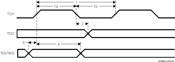
Table 5-27 Switching Characteristics Over Recommended Operating Conditions for IEEE 1149.1 JTAG

NO. PARAMETER MIN TYP MAX UNIT
2 td(TCKL-TDOV) Delay time, TCK low to TDO valid 0 25 ns
IWR1642 SPRS91v_JTAG_01.gifFigure 5-20 JTAG Timing