JAJSUK0 May 2024 IWR2944
PRODUCTION DATA
- 1
- 1 特長
- 2 アプリケーション
- 3 概要
- 4 Device Comparison
- 5 Pin Configurations and Functions
-
6 Specifications
- 6.1 Absolute Maximum Ratings
- 6.2 ESD Ratings
- 6.3 Power-On Hours (POH)
- 6.4 Recommended Operating Conditions
- 6.5 VPP Specifications for One-Time Programmable (OTP) eFuses
- 6.6 Power Supply Specifications
- 6.7 Power Consumption Summary
- 6.8 RF Specifications
- 6.9 Thermal Resistance Characteristics
- 6.10 Power Supply Sequencing and Reset Timing
- 6.11 Input Clocks and Oscillators
- 6.12
Peripheral Information
- 6.12.1
QSPI Flash Memory Peripheral
- 6.12.1.1 QSPI Timing Conditions
- 6.12.1.2 QSPI Timing Requirements #GUID-CD30070D-F132-4A2C-92CD-5AA96AE70B94/GUID-97D19708-D87E-443B-9ADF-1760CFEF6F4C #GUID-CD30070D-F132-4A2C-92CD-5AA96AE70B94/GUID-0A61EEC9-2B95-4C27-B219-18D27C8F9430
- 6.12.1.3 QSPI Switching Characteristics #GUID-20B35D26-AFE6-451C-B9E9-B3F2FA08097C/T4362547-64 #GUID-20B35D26-AFE6-451C-B9E9-B3F2FA08097C/T4362547-65
- 6.12.2
Multibuffered / Standard Serial Peripheral Interface (MibSPI)
- 6.12.2.1 MibSPI Peripheral Description
- 6.12.2.2
MibSPI Transmit and Receive RAM Organization
- 6.12.2.2.1 SPI Timing Conditions
- 6.12.2.2.2 SPI Controller Mode Switching Parameters (CLOCK PHASE = 0, SPICLK = output, SPISIMO = output, and SPISOMI = input) #GUID-20BA2ACF-4FC2-43F6-960F-1A4CA56E65A6/T4362547-236 #GUID-20BA2ACF-4FC2-43F6-960F-1A4CA56E65A6/T4362547-237 #GUID-20BA2ACF-4FC2-43F6-960F-1A4CA56E65A6/T4362547-238
- 6.12.2.2.3 SPI Controller Mode Switching Parameters (CLOCK PHASE = 1, SPICLK = output, SPISIMO = output, and SPISOMI = input) #GUID-517E5284-3345-461F-B07F-EB95741B1272/T4362547-244 #GUID-517E5284-3345-461F-B07F-EB95741B1272/T4362547-245 #GUID-517E5284-3345-461F-B07F-EB95741B1272/T4362547-246
- 6.12.2.3 SPI Peripheral Mode I/O Timings
- 6.12.3
Ethernet Switch (RGMII/RMII/MII)
Peripheral
- 6.12.3.1 RGMII/MII Timing Conditions
- 6.12.3.2 RGMII Transmit Clock Switching Characteristics
- 6.12.3.3 RGMII Transmit Data and Control Switching Characteristics
- 6.12.3.4 RGMII Receive Clock Timing Requirements
- 6.12.3.5 RGMII Receive Data and Control Timing Requirements
- 6.12.3.6 RMII Transmit Clock Switching Characteristics
- 6.12.3.7 RMII Transmit Data and Control Switching Characteristics
- 6.12.3.8 RMII Receive Clock Timing Requirements
- 6.12.3.9 RMII Receive Data and Control Timing Requirements
- 6.12.3.10 MII Transmit Switching Characteristics
- 6.12.3.11 MII Receive Clock Timing Requirements
- 6.12.3.12 MII Receive Timing Requirements
- 6.12.3.13 MII Transmit Clock Timing Requirements
- 6.12.3.14 MDIO Interface Timings
- 6.12.4 LVDS/Aurora Instrumentation and Measurement Peripheral
- 6.12.5 UART Peripheral
- 6.12.6 Inter-Integrated Circuit Interface (I2C)
- 6.12.7 Controller Area Network - Flexible Data-rate (CAN-FD)
- 6.12.8 CSI2 Receiver Peripheral
- 6.12.9 Enhanced Pulse-Width Modulator (ePWM)
- 6.12.10 General-Purpose Input/Output
- 6.12.1
QSPI Flash Memory Peripheral
- 6.13 Emulation and Debug
- 7 Detailed Description
- 8 Monitoring and Diagnostics
- 9 Applications, Implementation, and Layout
- 10デバイスおよびドキュメントのサポート
- 11Revision History
- 12Mechanical, Packaging, and Orderable Information
7.3.1.2 Transmit Subsystem
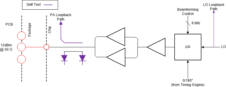
The device transmit subsystem consists of four parallel transmit chains, each with independent phase and amplitude control. All four transmitters can be used simultaneously or in time-multiplexed fashion. The device supports binary phase modulation and a 6 bit programmable phase shifter for beamforming control on a per chirp basis for each channel as indicated in the figure below.
Each transmit chain can deliver a maximum of 12 dBm at the antenna port on the PCB. The transmit chains also support programmable backoff for system optimization.
Figure 7-3 describes the transmit subsystem.
 Figure 7-3 Transmit Subsystem (Per Channel)