JAJSPG2A December 2022 – March 2024 IWRL6432
PRODUCTION DATA
- 1
- 1 特長
- 2 アプリケーション
- 3 概要
- 4 機能ブロック図
- 5 Device Comparison
- 6 Terminal Configurations and Functions
-
7 Specifications
- 7.1 Absolute Maximum Ratings
- 7.2 ESD Ratings
- 7.3 Power-On Hours (POH)
- 7.4 Recommended Operating Conditions
- 7.5 VPP Specifications for One-Time Programmable (OTP) eFuses
- 7.6
Power Supply Specifications
- 7.6.1 Power Optimized 3.3V I/O Topology
- 7.6.2 BOM Optimized 3.3V I/O Topology
- 7.6.3 Power Optimized 1.8V I/O Topology
- 7.6.4 BOM Optimized 1.8V I/O Topology
- 7.6.5 System Topologies
- 7.6.6 Internal LDO output decoupling capacitor and layout conditions for BOM optimized topology
- 7.6.7 Noise and Ripple Specifications
- 7.7 Power Save Modes
- 7.8 Peak Current Requirement per Voltage Rail
- 7.9 RF Specification
- 7.10 Supported DFE Features
- 7.11 CPU Specifications
- 7.12 Thermal Resistance Characteristics
- 7.13
Timing and Switching Characteristics
- 7.13.1 Power Supply Sequencing and Reset Timing
- 7.13.2 Synchronized Frame Triggering
- 7.13.3 Input Clocks and Oscillators
- 7.13.4 MultiChannel buffered / Standard Serial Peripheral Interface (McSPI)
- 7.13.5 RDIF Interface Configuration
- 7.13.6 General-Purpose Input/Output
- 7.13.7 Controller Area Network - Flexible Data-rate (CAN-FD)
- 7.13.8 Serial Communication Interface (SCI)
- 7.13.9 Inter-Integrated Circuit Interface (I2C)
- 7.13.10 Quad Serial Peripheral Interface (QSPI)
- 7.13.11 JTAG Interface
-
8 Detailed Description
- 8.1 Overview
- 8.2 機能ブロック図
- 8.3 Subsystems
- 8.4 Other Subsystems
- 8.5 Memory Partitioning Options
- 8.6 Boot Modes
- 9 Monitoring and Diagnostics
- 10Applications, Implementation, and Layout
- 11Device and Documentation Support
- 12Revision History
- 13Mechanical, Packaging, and Orderable Information
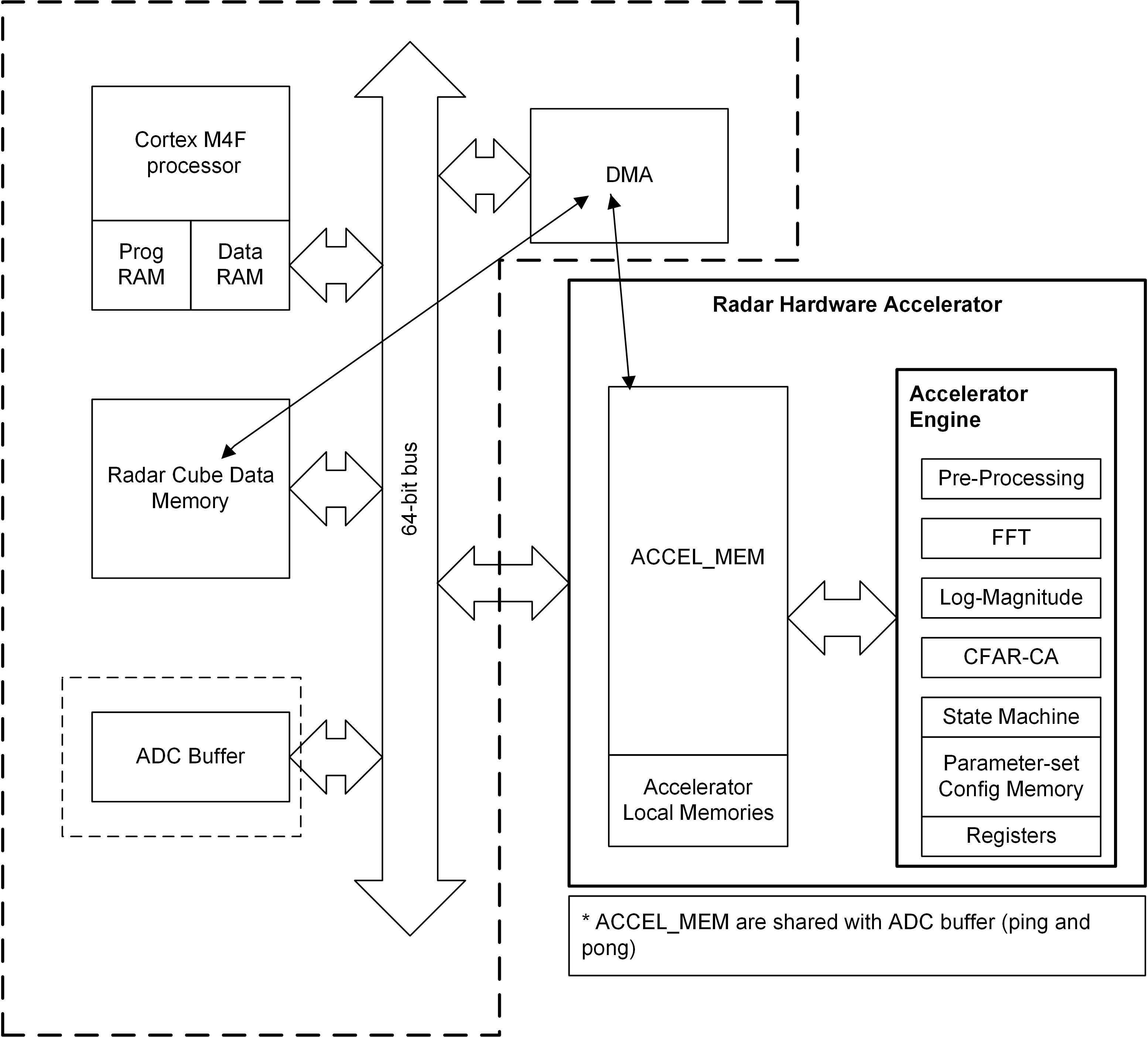
8.3.8 Hardware Accelerator (HWA1.2) Features
- Fast FFT computation, with programmable 2N sizes, up to 1024-point complex FFT
- Internal FFT bit-width of 24 bits (each for I and Q) for good Signal-to-Quantization-Noise Ratio (SQNR) performance
- Fully programmable butterfly scaling at every radix-2 stage for user flexibility
- Built-in capabilities for pre-FFT processing – Ex: DC estimation and subtraction
- DC estimation & subtraction, Interference estimation & zero-out, Real window, Complex pre-multiplication
- Magnitude (absolute value) and Log-magnitude computation
- Flexible data flow and data sample arrangement to support efficient multi-dimensional FFT operations and transpose accesses
- Chaining and looping mechanism to sequence a set of operations one after another with minimal intervention from the main processor
- Peak detection – CFAR (CFAR-CA, CFAR-OS) detector
- Basic statistics, including Sum and 1D Max
- Compression engine for radar cube memory optimization
 Figure 8-6 HWA 1.2 Functional Block
Diagram