SWRS311 December   2024 IWRL6432W

PRODUCTION DATA  

  1.   1
  2. Features
  3. Applications
  4. Description
  5. Functional Block Diagram
  6. Device Comparison
    1. 5.1 Related Products
  7. Terminal Configurations and Functions
    1. 6.1 Pin Diagrams
    2. 6.2 Signal Descriptions
      1.      11
      2.      12
      3.      13
      4.      14
      5.      15
      6.      16
      7.      17
      8.      18
      9.      19
      10.      20
      11.      21
      12.      22
      13.      23
      14.      24
      15.      25
      16.      26
      17.      27
    3.     28
  8. Specifications
    1. 7.1  Absolute Maximum Ratings
    2. 7.2  ESD Ratings
    3. 7.3  Power-On Hours (POH)
    4. 7.4  Recommended Operating Conditions
    5. 7.5  VPP Specifications for One-Time Programmable (OTP) eFuses
      1. 7.5.1 Recommended Operating Conditions for OTP eFuse Programming
      2. 7.5.2 Hardware Requirements
      3. 7.5.3 Impact to Your Hardware Warranty
    6. 7.6  Power Supply Specifications
      1. 7.6.1 Power Optimized 3.3V I/O Topology
      2. 7.6.2 BOM Optimized 3.3V I/O Topology
      3. 7.6.3 Power Optimized 1.8V I/O Topology
      4. 7.6.4 BOM Optimized 1.8V I/O Topology
      5. 7.6.5 System Topologies
        1. 7.6.5.1 Power Topologies
          1. 7.6.5.1.1 BOM Optimized Mode
          2. 7.6.5.1.2 Power Optimized Mode
      6. 7.6.6 Internal LDO output decoupling capacitor and layout conditions for BOM optimized topology
        1. 7.6.6.1 Single-Capacitor Rail
          1. 7.6.6.1.1 1.2V Digital LDO
        2. 7.6.6.2 Two-capacitor rail
          1. 7.6.6.2.1 1.2V RF LDO
          2. 7.6.6.2.2 1.2V SRAM LDO
          3. 7.6.6.2.3 1.0V RF LDO
      7. 7.6.7 Noise and Ripple Specifications
    7. 7.7  Power Save Modes
      1. 7.7.1 Typical Power Consumption Numbers
    8. 7.8  Peak Current Requirement per Voltage Rail
    9. 7.9  RF Specification
    10. 7.10 Supported DFE Features
    11. 7.11 CPU Specifications
    12. 7.12 Thermal Resistance Characteristics
    13. 7.13 Timing and Switching Characteristics
      1. 7.13.1  Power Supply Sequencing and Reset Timing
      2. 7.13.2  Synchronized Frame Triggering
      3. 7.13.3  Input Clocks and Oscillators
        1. 7.13.3.1 Clock Specifications
      4. 7.13.4  MultiChannel buffered / Standard Serial Peripheral Interface (McSPI)
        1. 7.13.4.1 McSPI Features
        2. 7.13.4.2 SPI Timing Conditions
        3. 7.13.4.3 SPI—Controller Mode
          1. 7.13.4.3.1 Timing and Switching Requirements for SPI - Controller Mode
          2. 7.13.4.3.2 Timing and Switching Characteristics for SPI Output Timings—Controller Mode
        4. 7.13.4.4 SPI—Peripheral Mode
          1. 7.13.4.4.1 Timing and Switching Requirements for SPI - Peripheral Mode
          2. 7.13.4.4.2 Timing and Switching Characteristics for SPI Output Timings—Secondary Mode
      5. 7.13.5  RDIF Interface Configuration
        1. 7.13.5.1 RDIF Interface Timings
        2. 7.13.5.2 RDIF Data Format
      6. 7.13.6  General-Purpose Input/Output
        1. 7.13.6.1 Switching Characteristics for Output Timing versus Load Capacitance (CL)
      7. 7.13.7  Controller Area Network - Flexible Data-rate (CAN-FD)
        1. 7.13.7.1 Dynamic Characteristics for the CANx TX and RX Pins
      8. 7.13.8  Serial Communication Interface (SCI)
        1. 7.13.8.1 SCI Timing Requirements
      9. 7.13.9  Inter-Integrated Circuit Interface (I2C)
        1. 7.13.9.1 I2C Timing Requirements
      10. 7.13.10 Quad Serial Peripheral Interface (QSPI)
        1. 7.13.10.1 QSPI Timing Conditions
        2. 7.13.10.2 Timing Requirements for QSPI Input (Read) Timings
        3. 7.13.10.3 QSPI Switching Characteristics
      11. 7.13.11 JTAG Interface
        1. 7.13.11.1 JTAG Timing Conditions
        2. 7.13.11.2 Timing Requirements for IEEE 1149.1 JTAG
        3. 7.13.11.3 Switching Characteristics Over Recommended Operating Conditions for IEEE 1149.1 JTAG
  9. Detailed Description
    1. 8.1 Overview
    2. 8.2 Functional Block Diagram
    3. 8.3 Subsystems
      1. 8.3.1 RF and Analog Subsystem
      2. 8.3.2 Clock Subsystem
      3. 8.3.3 Transmit Subsystem
      4. 8.3.4 Receive Subsystem
      5. 8.3.5 Processor Subsystem
      6. 8.3.6 Host Interface
      7. 8.3.7 Application Subsystem Cortex-M4F
      8. 8.3.8 Hardware Accelerator (HWA1.2) Features
        1. 8.3.8.1 Hardware Accelerator Feature Differences Between HWA1.1 and HWA1.2
    4. 8.4 Other Subsystems
      1. 8.4.1 GPADC Channels (Service) for User Application
      2. 8.4.2 GPADC Parameters
    5. 8.5 Memory Partitioning Options
    6. 8.6 Boot Modes
  10. Applications, Implementation, and Layout
    1. 9.1 Application Information
  11. 10Device and Documentation Support
    1. 10.1 Device Nomenclature
    2. 10.2 Tools and Software
    3. 10.3 Documentation Support
    4. 10.4 Support Resources
    5. 10.5 Trademarks
    6. 10.6 Electrostatic Discharge Caution
    7. 10.7 Glossary
  12. 11Revision History
  13. 12Mechanical, Packaging, and Orderable Information

パッケージ・オプション

メカニカル・データ(パッケージ|ピン)
  • YFF|111
サーマルパッド・メカニカル・データ
発注情報
Power Optimized Mode

This mode is designed for applications needing ultra-low power applications. The device can either be powered using two rails (1.8V and 1.2V) or with three rails (3.3V, 1.8V and 1.2V).
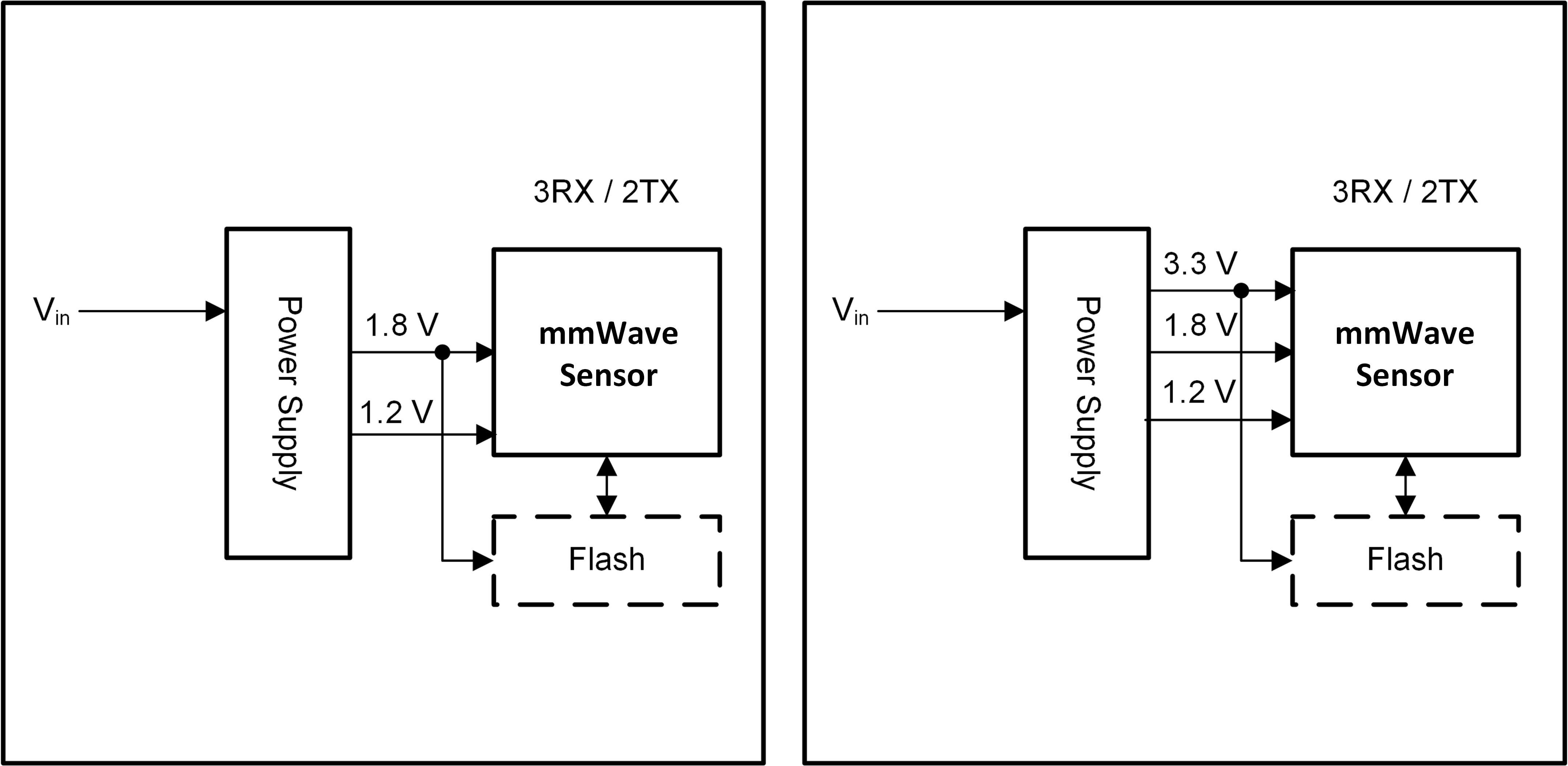
IWRL6432W Power Optimized Mode Power Management (Left: 1.8V I/O Topology, Right: 3.3V I/O Topology)Figure 7-3 Power Optimized Mode Power Management (Left: 1.8V I/O Topology, Right: 3.3V I/O Topology)