SWRS311 December 2024 IWRL6432W
PRODUCTION DATA
- 1
- 1 Features
- 2 Applications
- 3 Description
- 4 Functional Block Diagram
- 5 Device Comparison
- 6 Terminal Configurations and Functions
-
7 Specifications
- 7.1 Absolute Maximum Ratings
- 7.2 ESD Ratings
- 7.3 Power-On Hours (POH)
- 7.4 Recommended Operating Conditions
- 7.5 VPP Specifications for One-Time Programmable (OTP) eFuses
- 7.6
Power Supply
Specifications
- 7.6.1 Power Optimized 3.3V I/O Topology
- 7.6.2 BOM Optimized 3.3V I/O Topology
- 7.6.3 Power Optimized 1.8V I/O Topology
- 7.6.4 BOM Optimized 1.8V I/O Topology
- 7.6.5 System Topologies
- 7.6.6 Internal LDO output decoupling capacitor and layout conditions for BOM optimized topology
- 7.6.7 Noise and Ripple Specifications
- 7.7 Power Save Modes
- 7.8 Peak Current Requirement per Voltage Rail
- 7.9 RF Specification
- 7.10 Supported DFE Features
- 7.11 CPU Specifications
- 7.12 Thermal Resistance Characteristics
- 7.13
Timing and Switching
Characteristics
- 7.13.1 Power Supply Sequencing and Reset Timing
- 7.13.2 Synchronized Frame Triggering
- 7.13.3 Input Clocks and Oscillators
- 7.13.4 MultiChannel buffered / Standard Serial Peripheral Interface (McSPI)
- 7.13.5 RDIF Interface Configuration
- 7.13.6 General-Purpose Input/Output
- 7.13.7 Controller Area Network - Flexible Data-rate (CAN-FD)
- 7.13.8 Serial Communication Interface (SCI)
- 7.13.9 Inter-Integrated Circuit Interface (I2C)
- 7.13.10 Quad Serial Peripheral Interface (QSPI)
- 7.13.11 JTAG Interface
-
8 Detailed Description
- 8.1 Overview
- 8.2 Functional Block Diagram
- 8.3 Subsystems
- 8.4 Other Subsystems
- 8.5 Memory Partitioning Options
- 8.6 Boot Modes
- 9 Applications, Implementation, and Layout
- 10Device and Documentation Support
- 11Revision History
- 12Mechanical, Packaging, and Orderable Information
7.9 RF Specification
Over recommended operating
conditions (unless otherwise noted)
| PARAMETER | MIN | TYP | MAX | UNIT | ||
|---|---|---|---|---|---|---|
| Receiver | Noise figure | 57 to 63.9GHz | 12 | dB | ||
| 1-dB compression point (Out Of Band)(1) | –9 | dBm | ||||
| Maximum gain | 40 | dB | ||||
| Gain range | 10 | dB | ||||
| Gain step size | 2 | dB | ||||
| IF bandwidth(2) | 5 | MHz | ||||
| ADC sampling rate (real) | 12.5 | Msps | ||||
| ADC resolution | 12 | Bits | ||||
| S11(3) | -8 | dB | ||||
| Transmitter | Output Power | 10 | dBm | |||
| Power backoff range | 15 | dB | ||||
| S11(3) | -8 | dB | ||||
| Clock subsystem | Frequency range | 57 | 63.9 | GHz | ||
| Ramp rate | 400 | MHz/µs | ||||
| Phase noise at 1MHz offset | 57 to 63.9GHz | –89 | dBc/Hz | |||
(1) 1-dB Compression Point (Out Of Band) is measured by feed a Continuous wave Tone
well below the lowest HPF cut-off frequency.
(2) The analog IF stages include high-pass filtering, with configurable first-order
high-pass corner frequency. The set of available HPF corners is summarized as
follows:
The filtering performed by the digital baseband chain is targeted to
provide less than ±0.5dB pass-band ripple/droop.
| Available HPF Corner Frequencies (kHz) |
| 175, 350, 700, 1400 |
(3) RX3 and TX1 channels show
degraded S11 (-5.5dB) compared to the rest of the channels due to impedance
mismatch in the die to package transition.
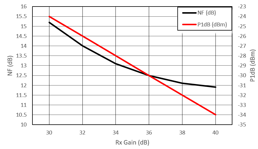
Figure 7-6 shows variations of noise figure and in-band P1dB parameters with respect to receiver gain programmed.
 Figure 7-6 Noise Figure, In-band P1dB vs
Receiver Gain