SNOSCZ6 April 2016 LDC1312-Q1 , LDC1314-Q1
PRODUCTION DATA.
- 1 Features
- 2 Applications
- 3 Description
- 4 Revision History
- 5 Description Continued
- 6 Pin Configuration and Functions
- 7 Specifications
-
8 Detailed Description
- 8.1 Overview
- 8.2 Functional Block Diagram
- 8.3 Feature Description
- 8.4 Device Functional Modes
- 8.5 Programming
- 8.6
Register Maps
- 8.6.1 Register List
- 8.6.2 Address 0x00, DATA_CH0
- 8.6.3 Address 0x02, DATA_CH1
- 8.6.4 Address 0x04, DATA_CH2 (LDC1314 only)
- 8.6.5 Address 0x06, DATA_CH3 (LDC1314 only)
- 8.6.6 Address 0x08, RCOUNT_CH0
- 8.6.7 Address 0x09, RCOUNT_CH1
- 8.6.8 Address 0x0A, RCOUNT_CH2 (LDC1314 only)
- 8.6.9 Address 0x0B, RCOUNT_CH3 (LDC1314 only)
- 8.6.10 Address 0x0C, OFFSET_CH0
- 8.6.11 Address 0x0D, OFFSET_CH1
- 8.6.12 Address 0x0E, OFFSET_CH2 (LDC1314 only)
- 8.6.13 Address 0x0F, OFFSET_CH3 (LDC1314 only)
- 8.6.14 Address 0x10, SETTLECOUNT_CH0
- 8.6.15 Address 0x11, SETTLECOUNT_CH1
- 8.6.16 Address 0x12, SETTLECOUNT_CH2 (LDC1314 only)
- 8.6.17 Address 0x13, SETTLECOUNT_CH3 (LDC1314 only)
- 8.6.18 Address 0x14, CLOCK_DIVIDERS_CH0
- 8.6.19 Address 0x15, CLOCK_DIVIDERS_CH1
- 8.6.20 Address 0x16, CLOCK_DIVIDERS_CH2 (LDC1314 only)
- 8.6.21 Address 0x17, CLOCK_DIVIDERS_CH3 (LDC1314 only)
- 8.6.22 Address 0x18, STATUS
- 8.6.23 Address 0x19, ERROR_CONFIG
- 8.6.24 Address 0x1A, CONFIG
- 8.6.25 Address 0x1B, MUX_CONFIG
- 8.6.26 Address 0x1C, RESET_DEV
- 8.6.27 Address 0x1E, DRIVE_CURRENT_CH0
- 8.6.28 Address 0x1F, DRIVE_CURRENT_CH1
- 8.6.29 Address 0x20, DRIVE_CURRENT_CH2 (LDC1314 only)
- 8.6.30 Address 0x21, DRIVE_CURRENT_CH3 (LDC1314 only)
- 8.6.31 Address 0x7E, MANUFACTURER_ID
- 8.6.32 Address 0x7F, DEVICE_ID
- 9 Application and Implementation
- 10Power Supply Recommendations
- 11Layout
- 12Device and Documentation Support
- 13Mechanical, Packaging, and Orderable Information
6 Pin Configuration and Functions
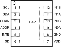
LDC1312-Q1 DNT
12 pin WSON
Top View

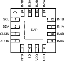
LDC1314-Q1 RGH
16 pin WQFN
Top View

Pin Functions
| PIN | TYPE(1) | DESCRIPTION | |
|---|---|---|---|
| NO. | NAME | ||
| 1 | SCL | I | I2C Clock input |
| 2 | SDA | I/O | I2C Data input/output |
| 3 | CLKIN | I | Master Clock input. Tie this pin to GND if internal oscillator is selected |
| 4 | ADDR | I | I2C Address selection pin: when ADDR=L, I2C address = 0x2A, when ADDR=H, I2C address = 0x2B. |
| 5 | INTB | O | Configurable Interrupt output pin |
| 6 | SD | I | Shutdown input |
| 7 | VDD | P | Power Supply |
| 8 | GND | G | Ground |
| 9 | IN0A | A | External LC sensor 0 connection |
| 10 | IN0B | A | External LC sensor 0 connection |
| 11 | IN1A | A | External LC sensor 1 connection |
| 12 | IN1B | A | External LC sensor 1 connection |
| 13 | IN2A | A | External LC sensor 2 connection (LDC1314 only) |
| 14 | IN2B | A | External LC sensor 2 connection (LDC1314 only) |
| 15 | IN3A | A | External LC sensor 3 connection (LDC1314 only) |
| 16 | IN3B | A | External LC sensor 3 connection (LDC1314 only) |
| DAP | DAP(2) | N/A | Connect to Ground |
(1) I = Input, O = Output, P=Power, G=Ground, A=Analog
(2) There is an internal electrical connection between the exposed Die Attach Pad (DAP) and the GND pin of the device. Although the DAP can be left floating, for best performance the DAP should be connected to the same potential as the device's GND pin. Do not use the DAP as the primary ground for the device. The device GND pin must always be connected to ground.